AP1084T25G-13(2007) Ver la hoja de datos (PDF) - Diodes Incorporated.
Número de pieza
componentes Descripción
Lista de partido
AP1084T25G-13
(Rev.:2007)
(Rev.:2007)
Diodes Incorporated.

AP1084T25G-13 Datasheet PDF : 10 Pages
| |||
AP1084
5A LOW DROPOUT POSITIVE ADJUSTABLE OR
FIXED-MODE REGULATOR
Electrical Characteristics (Under Operating Conditions)
Sym.
Parameter
Conditions
Min. Typ. Max. Unit
VREF Reference Voltage
AP1084-XXX
AP1084-1.5
Line AP1084-1.8
Regula
tion
AP1084-2.5
AP1084-3.3
AP1084-5.0
AP1084-Adj
AP1084-1.5
Io = 10mA, TA = 25oC, (Vin-Vout) = 1.5V
IO = 10mA, VOUT+1.5V<VIN<12V, TA = 25oC
IOUT = 10mA, TA = 25oC, 3V≦VIN≦12V
IOUT = 10mA, TA = 25oC, 3.3V≦VIN≦12V
IOUT = 10mA, TA = 25oC, 4V≦VIN≦12V
IOUT = 10mA, TA = 25oC, 4.8V≦VIN≦12V
IOUT = 10mA, TA = 25oC, 6.5V≦VIN≦12V
VIN = 3.3V, 0mA<Io<5A, TA = 25oC
C
VIN = 3V, 0mA<Io<5A, TA = 25oC
(Note 4, 5)
1.225
1.470
1.764
2.450
3.235
4.900
Load AP1084-1.8
Regula
tion AP1084-2.5
AP1084-3.3
AP1084-5.0
VIN = 3.3V, 0mA<Io<5A
TA = 25oC (Note 4, 5)
VIN = 4V, 0mA < Io < 5A
TA = 25oC (Note 4, 5)
VIN = 5V, 0mA < Io < 5A, TA = 25oC
(Note 4, 5)
VIN = 8V, 0mA < Io < 5A, TA = 25oC
(Note 4, 5)
∆Vo Dropout Voltage Io = 5.0A (∆Vout = 1% Vout)
Current Limit
Vin-Vout = 5V
5.1
Minimum Load
Current
Temperature
Stability
Io = 10mA
θJA
Thermal Resistance
Junction-to-Ambient
(No heat sink; No
air flow)
TO252-3L
TO263-3L
TO220-3L
θJC
Thermal Resistance
Junction-to-Case
TO252-3L:
TO263-3L:
TO220-3L:
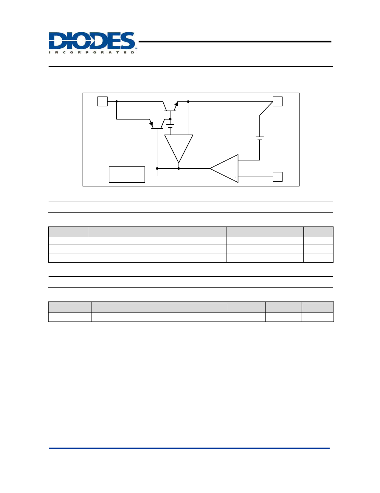
Control
Control
Control
Circuitry/Power
Circuitry/Power
Circuitry/Power
Transistor
Transistor
Transistor
1.250
1.500
1.800
2.500
3.300
5.000
12
15
20
26
40
1.3
5
0.5
98
95
83
10
19
13
1.275 V
0.2
%
1.530 V
1.836 V
2.550 V
3.365 V
5.100 V
1
%
15
mV
18
mV
25
mV
33
mV
50
mV
1.4
V
A
10
mA
%
OC/W
OC/W
Note:
4. See thermal regulation specifications for changes in output voltage due to heating effects. Line and load regulation are measured at a constant
junction temperature by low duty cycle pulse testing. Load regulation is measured at the output lead = 1/18” from the package.
5. Line and load regulation are guaranteed up to the maximum power dissipation of 15W. Power dissipation is determined by the difference between
input and output and the output current. Guaranteed maximum power dissipation will not be available over the full input/output range.
AP1084 Rev. 1
4 of 10
www.diodes.com
FEBRUARY 2007
© Diodes Incorporated
Share Link: