PI74LPT16373 Ver la hoja de datos (PDF) - Pericom Semiconductor
Número de pieza
componentes Descripción
Lista de partido
PI74LPT16373 Datasheet PDF : 5 Pages
| |||
PI74LPT16373
123456789012345678901234567890121234567890123456789012345678901212345678901234567890123345.367V89011261-2B34I5T678T90R123A45N67S89P01A23R45E67N890T121L23A45T67C89H012
PI74LPT16373 1122334455667788990011223344556677889900112233445566778899001122112233445566778899001122334455667788990011223344556677889900112211223344556677889900112233445566778899001122334455667788990011221122334455667788990011223344556677889900112233445566778899001122112233445566778899001122
Fast CMOS 3.3V 16-Bit 1
Transparent Latch
Product Features
• Compatible with LCX™ and LVT™ families of products
Product Description
2
Pericom Semiconductor’s PI74LPT series of logic circuits are pro-
• Supports 5V Tolerant Mixed Signal Mode Operation
duced in the Company’s advanced 0.6 micron CMOS technology,
– Input can be 3V or 5V
achieving industry leading speed grades.
– Output can be 3V or connected to 5V bus
• Advanced Low Power CMOS Operation
3 The PI74LPT16373 is a 16-bit transparent latch designed with
3-state outputs and are intended for bus oriented applications. The
• Excellent output drive capability:
Output Enable and Latch Enable controls are organized to operate
Balanced drives (24 mA sink and source)
as two 8-bit latches or one 16-bit latch. When Latch Enable (LE) is
• Pin compatible with industry standard double-density
pinouts
• Low ground bounce outputs
• Hysteresis on all inputs
• Industrial operating temperature range: –40°C to +85°C
4 HIGH, the flip-flops appear transparent to the data. The data that
meets the set-up time when LE is LOW is latched. When OE is
HIGH, the bus output is in the high impedance state.
5 The PI74LPT16373 can be driven from either 3.3V or 5.0V devices
allowing this device to be used as a translator in a mixed
3.3/5.0V system.
• Multiple center pins and distributed Vcc/GND pins
minimize switching noise
• Packages available:
6
– 48-pin 240 mil wide thin plastic TSSOP (A)
– 48-pin 300 mil wide plastic SSOP (V)
7
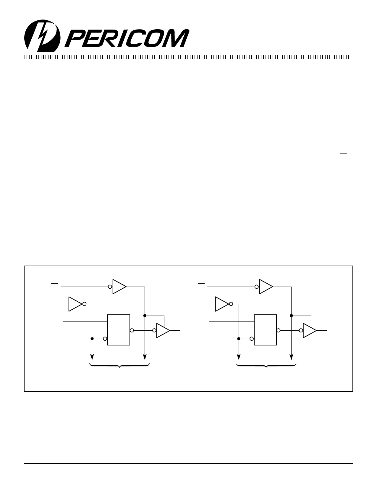
Logic Block Diagram
8
1OE
1LE
1D0
D
C
2OE
2LE
2D0
D
1O0
C
9
10
2O0
11
12
TO 7 OTHER CHANNELS
TO 7 OTHER CHANNELS
13
14
15
1
PS2069A 01/16/97
Share Link: 