DM9102D Ver la hoja de datos (PDF) - Davicom Semiconductor, Inc.
Número de pieza
componentes Descripción
Lista de partido
DM9102D Datasheet PDF : 70 Pages
| |||
37
TEST1
94
WOL
97
X2
98
X1/OSC
102
BGRES
116
ISOLATE#
95
VCTRL25
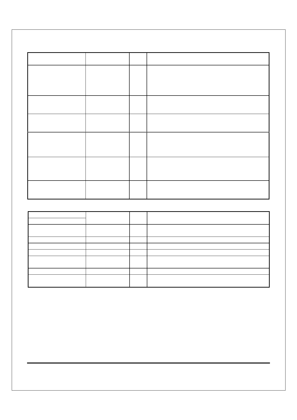
5.6 Power Pins
Pin No.
128LQFP
101
100,107,108
103,104,111,112
96
8,9,15,22,28,29,35,45,
46,58,76,86,99,125
82,120
4,5,12,18,19,25,32,42,52,
53,61,70
Pin Name
BGRESG
AGND
AVDD25
AVDD
DGND
DVDD25
DVDD
I TEST Mode Control 1
In normal operation, tie low to this pin.
O Wake up signal.
The DM9102D can assert this pin if it detects link status
change, magic packet, or sample frame match. The default is
low active pulse mode. The DM9102D also supports High/Low
and Pulse/Level options from EEPROM setting.
O Crystal feedback output
This pin is used for crystal connection only. Leave this pin open
if oscillator is used.
I Crystal or Oscillator Input. (25MHz±50ppm)
Connect to a 25MHz Oscillator or series resonance,
fundamental frequency crystal.
I Bandgap Voltage Reference Resistor.
It connects to a 6.8KΩ1% error tolerance resistor between this
pin and BGRESG pin, to provide an accurate current reference
for DM9102D (10Base-T/100Base-TX Application).
I Isolate
This pin is used to isolate the DM9102D from the PCI bus.
O Voltage 2.5V control
This pin can be used to control a BJT transistor ‘s base pin to
generate a stable 2.5V power in BJT’s drain pin .
I/O
Description
P Bandgap Ground
It is used together with the BGRES pin.
P Analog Ground
P Analog Power, +2.5V
P Analog Power, +3.3V
P Digital Ground
P Digital Power, +2.5V
P Digital Power, +3.3V
Final
9
Version: DM9102D-DS-F01
May 10, 2006
Share Link: 