FM25C160B Ver la hoja de datos (PDF) - Cypress Semiconductor
Número de pieza
componentes Descripción
Lista de partido
FM25C160B Datasheet PDF : 14 Pages
| |||
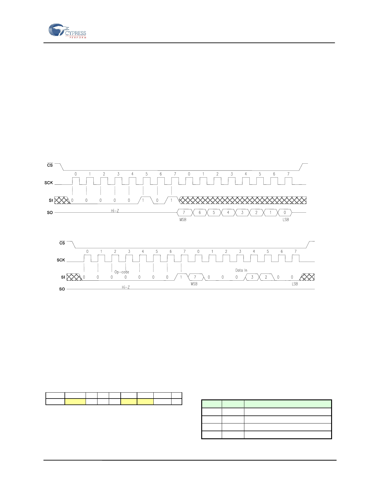
RDSR - Read Status Register
The RDSR command allows the bus master to verify
the contents of the Status register. Reading Status
provides information about the current state of the
write protection features. Following the RDSR op-
code, the FM25C160B will return one byte with the
contents of the Status register. The Status register is
described in detail in a later section.
FM25C160B - 16Kb 5V SPI F-RAM
WRSR – Write Status Register
The WRSR command allows the user to select
certain write protection features by writing a byte to
the Status register. Prior to issuing a WRSR
command, the /WP pin must be high or inactive. Note
that on the FM25C160B, /WP only prevents writing
to the Status register, not the memory array. Prior to
sending the WRSR command, the user must send a
WREN command to enable writes. Note that
executing a WRSR command is a write operation and
therefore clears the Write Enable Latch. The bus
timing for RDSR and WRSR are shown below.
Figure 7. RDSR Bus Timing
Figure 8. WRSR Bus Timing
Status Register & Write Protection
The write protection features of the FM25C160B are
multi-tiered. First, a WREN op-code must be issued
prior to any write operation. Assuming that writes are
enabled using WREN, writes to memory are
controlled by the Status register. As described above,
writes to the status register are performed using the
WRSR command and subject to the /WP pin. The
Status register is organized as follows.
Table 2. Status Register
Bit
7
654 3
2
10
Name WPEN 0 0 0 BP1 BP0 WEL 0
Bits 0 and 4-6 are fixed at 0 and cannot be modified.
Note that bit 0 (/RDY in EEPROMs) is wired low
since F-RAM writes have no delay and the memory
is never busy. All EEPROMs use Ready to indicate
whether a write cycle is complete or not. The WPEN,
BP1 and BP0 control write protection features. They
are nonvolatile (shaded yellow). The WEL flag
indicates the state of the Write Enable Latch. This bit
is internally set by the WREN command and is
cleared by terminating a write cycle (/CS high) or by
using the WRDI command.
BP1 and BP0 are memory block write protection bits.
They specify portions of memory that are write
protected as shown in the following table.
Table 3. Block Memory Write Protection
BP1 BP0 Protected Address Range
0
0 None
0
1 600h to 7FFh (upper ¼)
1
0 400h to 7FFh (upper ½)
1
1 000h to 7FFh (all)
Document Number: 001-84472 Rev. *A
Page 6 of 14
Share Link: 