HD74LVC2G53CLE Ver la hoja de datos (PDF) - Renesas Electronics
Número de pieza
componentes Descripción
Lista de partido
HD74LVC2G53CLE Datasheet PDF : 12 Pages
| |||
HD74LVC2G53
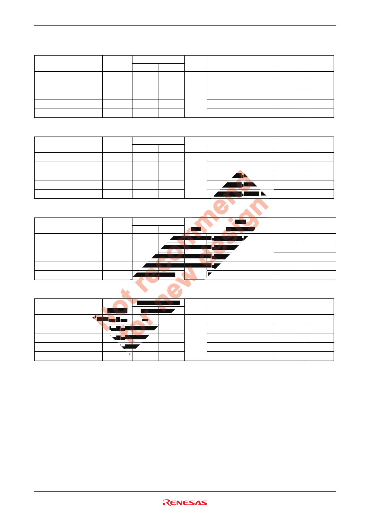
Switching Characteristics
• VCC = 1.8 ± 0.15 V
Item
Propagation delay time*1
Enable time
Disable time
Enable time
Disable time
Symbol
tPLH, tPHL
tZH, tZL
tHZ, tLZ
tZH, tZL
tHZ, tLZ
Ta = –40 to 85°C
Min
Max
2.0
3.3
9.0
3.2
10.9
2.9
10.3
2.1
9.4
Unit
ns
Test
Conditions
CL = 30 pF, RL = 1.0 kΩ
CL = 30 pF, RL = 1.0 kΩ
CL = 30 pF, RL = 1.0 kΩ
CL = 30 pF, RL = 1.0 kΩ
CL = 30 pF, RL = 1.0 kΩ
FROM
TO
(Input) (Output)
COM or Yn Yn or COM
INH
COM or Yn
INH
COM or Yn
A
Yn
A
Yn
• VCC = 2.5 ± 0.2 V
Item
Propagation delay time*1
Enable time
Disable time
Enable time
Disable time
Symbol
tPLH, tPHL
tZH, tZL
tHZ, tLZ
tZH, tZL
tHZ, tLZ
Ta = –40 to 85°C
Min
Max
1.2
2.5
6.1
2.3
9.3
2.1
7.2
1.4
7.9
Unit
ns
Test
Conditions
CL = 30 pF, RL = 500 Ω
CL = 30 pF, RL = 500 Ω
CL = 30 pF, RL = 500 Ω
CL = 30 pF, RL = 500 Ω
CL = 30 pF, RL = 500 Ω
FROM
TO
(Input) (Output)
COM or Yn Yn or COM
INH
COM or Yn
INH
COM or Yn
A
Yn
A
Yn
• VCC = 3.3 ± 0.3 V
Item
Propagation delay time*1
Enable time
Disable time
Enable time
Disable time
Symbol
tPLH, tPHL
tZH, tZL
tHZ, tLZ
tZH, tZL
tHZ, tLZ
Ta = –40 to 85°C
Min
Max
0.8
2.2
5.4
2.3
8.1
1.9
5.8
1.1
7.2
Unit
ns
Test
Conditions
CL = 50 pF, RL = 500 Ω
CL = 50 pF, RL = 500 Ω
CL = 50 pF, RL = 500 Ω
CL = 50 pF, RL = 500 Ω
CL = 50 pF, RL = 500 Ω
FROM
(Input)
TO
(Output)
COM or Yn Yn or COM
INH
COM or Yn
INH
COM or Yn
A
Yn
A
Yn
• VCC = 5.0 ± 0.5 V
Ta = –40 to 85°C
Test
FROM
TO
Item
Symbol Min
Propagation delay time*1 tPLH, tPHL
Max Unit
Conditions
(Input) (Output)
0.6
ns CL = 50 pF, RL = 500 Ω COM or Yn Yn or COM
Enable time
tZH, tZL
1.8
4.5
CL = 50 pF, RL = 500 Ω INH
COM or Yn
Disable time
tHZ, tLZ
1.6
8.0
CL = 50 pF, RL = 500 Ω INH
COM or Yn
Enable time
tZH, tZL
1.3
5.4
CL = 50 pF, RL = 500 Ω A
Yn
Disable time
tHZ, tLZ
1.0
5.0
CL = 50 pF, RL = 500 Ω A
Yn
Notes: 1. The propagation delay is calculated RC time constant of typical on-state resistance of the switch and the
specified load capacitance, when driven by an ideal voltage source (zero output impedance).
Rev.3.00 Jul 07, 2005 page 5 of 11
Share Link: 