LM293D Ver la hoja de datos (PDF) - Motorola => Freescale
Número de pieza
componentes Descripción
Lista de partido
LM293D Datasheet PDF : 6 Pages
| |||
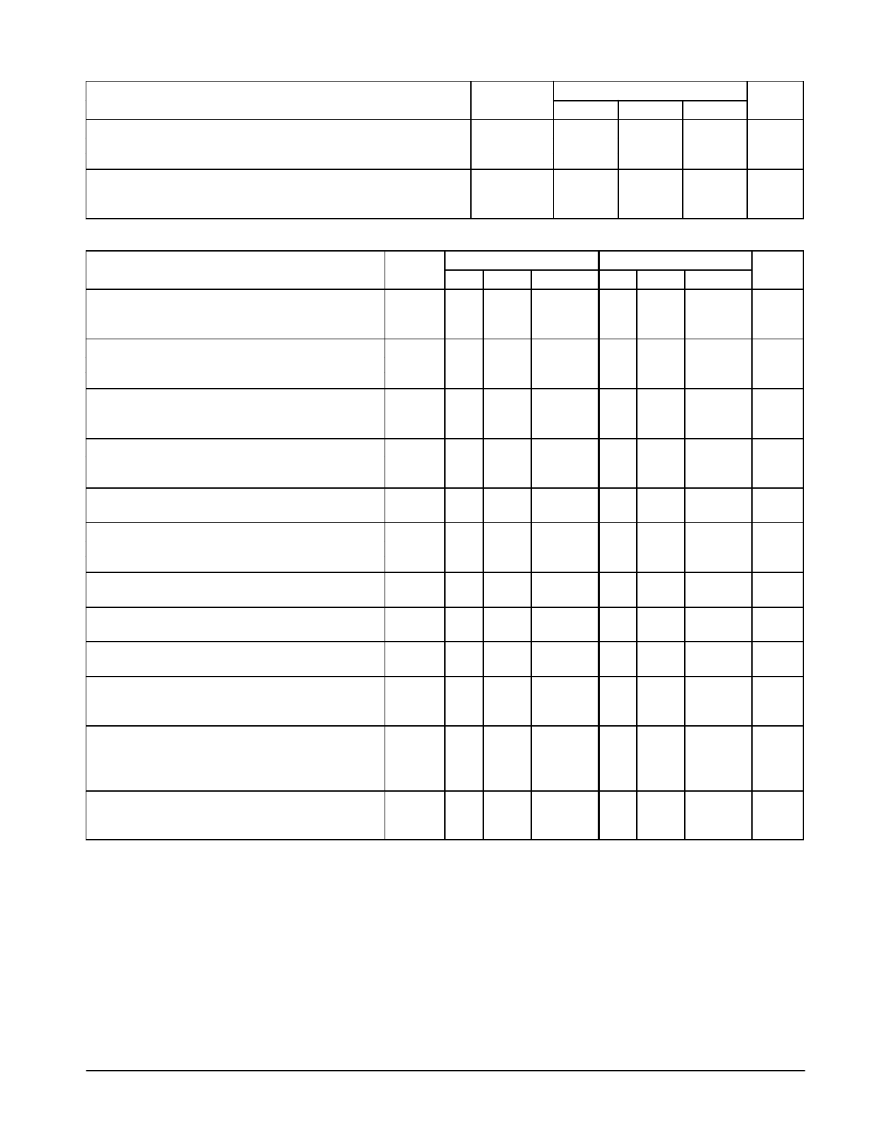
LM393, LM393A, LM293, LM2903, LM2903V
ELECTRICAL CHARACTERISTICS (VCC = 5.0 Vdc, Tlow ≤ TA ≤ Thigh,* unless otherwise noted.)
LM393A
Characteristic
Symbol
Min
Typ
Max
Unit
Output Leakage Current
Vin– = 0 V, Vin+ ≥ 1.0 Vdc, VO = 5.0 Vdc, TA= 25°C
Vin– = 0 V, Vin+ ≥ 1.0 Vdc, VO = 30 Vdc, Tlow ≤ TA ≤ Thigh
Supply Current
RL = ∞ Both Comparators, TA = 25°C
RL = ∞ Both Comparators, VCC = 30 V
IOL
µA
–
0.1
–
–
–
1.0
ICC
mA
–
0.4
1.0
–
1.0
2.5
ELECTRICAL CHARACTERISTICS (VCC = 5.0 Vdc, Tlow ≤ TA ≤ Thigh, unless otherwise noted.)
LM392, LM393
LM2903, LM2903V
Characteristic
Symbol Min Typ
Max
Min Typ
Max
Unit
Input Offset Voltage (Note 2)
TA = 25°C
Tlow ≤ TA ≤ Thigh
VIO
mV
–
±1.0
±5.0
–
±2.0
±7.0
–
–
9.0
–
9.0
15
Input Offset Current
TA = 25°C
Tlow ≤ TA ≤ Thigh
IIO
nA
–
±5.0
±50
–
±5.0
±50
–
–
±150
–
±50
±200
Input Bias Current (Note 3)
TA = 25°C
Tlow ≤ TA ≤ Thigh
IIB
nA
–
25
250
–
25
250
–
–
400
–
200
500
Input Common Mode Voltage Range (Note 3)
TA = 25°C
Tlow ≤ TA ≤ Thigh
Voltage Gain
RL ≥ 15 kΩ, VCC = 15 Vdc, TA = 25°C
VICR
0
0
–
VCC –1.5 0
–
VCC –2.0 0
V
–
VCC –1.5
–
VCC –2.0
AVOL
50
200
–
25 200
–
V/mV
Large Signal Response Time
Vin = TTL Logic Swing, Vref = 1.4 Vdc
VRL = 5.0 Vdc, RL = 5.1 kΩ, TA = 25°C
Response Time (Note 5)
VRL = 5.0 Vdc, RL = 5.1 kΩ, TA = 25°C
Input Differential Voltage (Note 6)
All Vin ≥ Gnd or V– Supply (if used)
–
–
300
–
–
300
–
ns
tTLH
–
1.3
–
–
1.5
–
µs
VID
–
–
VCC
–
–
VCC
V
Output Sink Current
ISink
6.0
16
–
6.0 16
–
mA
Vin ≥ 1.0 Vdc, Vin+ = 0 Vdc, VO ≤ 1.5 Vdc TA = 25°C
Output Saturation Voltage
VOL
mV
Vin ≥ 1.0 Vdc, Vin+ = 0, ISink ≤ 4.0 mA, TA = 25°C
–
150
400
–
–
400
Tlow ≤ TA ≤ Thigh
–
–
700
–
200
700
Output Leakage Current
IOL
nA
Vin– = 0 V, Vin+ ≥ 1.0 Vdc, VO = 5.0 Vdc, TA = 25°C
–
0.1
–
–
0.1
–
Vin– = 0 V, Vin+ ≥ 1.0 Vdc, VO = 30 Vdc,
Tlow ≤ TA ≤ Thigh
–
–
1000
–
–
1000
Supply Current
RL = ∞ Both Comparators, TA = 25°C
RL = ∞ Both Comparators, VCC = 30 V
ICC
mA
–
0.4
1.0
–
0.4
1.0
–
–
2.5
–
–
2.5
* Tlow = 0°C, Thigh = +70°C for LM393/393A
LM293 Tlow = –25°C, Thigh = +85°C
LM2903 Tlow = –40°C, Thigh = +105°C
] LM2903V Tlow = –40°C, Thigh = +125°C
NOTES: 2. At output switch point, VO 1.4 Vdc, RS = 0 Ω with VCC from 5.0 Vdc to 30 Vdc, and over the full input common mode range (0 V to VCC = –1.5 V).
3. Due to the PNP transistor inputs, bias current will flow out of the inputs. This current is essentially constant, independent of the output state, there
fore, no loading changes will exist on the input lines.
5. Response time is specified with a 100 mV step and 5.0 mV of overdrive. With larger magnitudes of overdrive faster response times are obtainable.
6. The comparator will exhibit proper output state if one of the inputs becomes greater than VCC, the other input must remain within the common mode
range. The low input state must not be less than –0.3 V of ground or minus supply.
MOTOROLA ANALOG IC DEVICE DATA
3
Share Link: 