MC10SX1125 Ver la hoja de datos (PDF) - ON Semiconductor
Número de pieza
componentes Descripción
Lista de partido
MC10SX1125 Datasheet PDF : 5 Pages
| |||
MC10SX1125
Coupling Capacitors
The SX1125 inputs must be AC coupled to allow proper
operation of the offset correction function. The coupling
capacitors, Cin, must be large enough to pass the lowest
input frequency of interest.
+ Cin
1
2p (Rin) (flow)
where
Rin = input resistance = 5000Ω
flow = lowest frequency.
Auto–zero Capacitors
A feedback amplifier is used to cancel the offset voltage of
the forward signal path, so the input to the internal ECL
comparator is at its toggle point in the absence of any input
signal. The time constant of the cancelling circuitry is set by
an external capacitor (CAZ) connected between Pins 1 and 2.
The formula for the calculation of the auto–zero capacitor is:
+ CAZ
150
2p (RAZ) (flow)
where
RAZ = internal driving impedance = 290kΩ
flow = lowest frequency.
Input Signal Level Detector
The SX1125 allows for user programmable input signal
level–detection and can automatically disable the switching
of its ECL data output if the input level is below a set
threshold. This prevents the outputs from reacting to noise in
the absence of a valid input signal, and ensures that data will
only be transmitted when the signal–to–noise ratio is
sufficient for low bit–error–rate system operation.
Complimentary ECL flags (LOS and LOSB) indicate whether
the input signal is above or below the desired threshold level.
In the level detect system, the input signal is amplified and
rectified before being compared to a programmable
reference. A filter is included to prevent noise spikes from
triggering the level–detector. The filter has a nominal 1µs
time constant, and additional filtering can be achieved by
using an external capacitor (CLD) from Pin 7 to VCCA (the
internal driving impedance is nominally 28k). The formula for
the calculation of the CLD capacitor is:
+ CLD
t
RZ
where
RZ = internal driving impedance = 28kΩ
t = LOS filter time constant.
DC CHARACTERISTICS (GNDA = GNDE = Ground; VCCA = VCCE = 4.5V to 5.5V)
Symbol
Characteristic
Min
Typ
Max
Unit
Condition
VIN
Input Signal Voltage (Din) Single-Ended
0.008
1.5
VP-P Note 1.
VOS
Input Offset Voltage
50
µV
VN
Input RMS Noise
225
µV
VTH
Input Level Detect Programmability
8.0
20
mVP-P
VHYS
Level Detect Hysteresis
1.5
2.5
7.0
dB
Note 2.
IIH
Input HIGH Current Disable
150
µA
ICC
Power Supply Current
33
45
mA
1. This device functions with Vinmin = 6mVP–P, but with increased BER (See BER data).
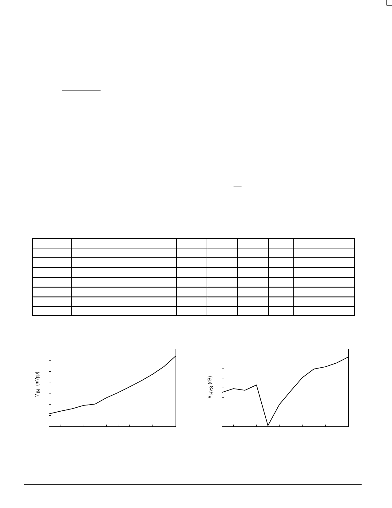
2. This device has an anomoly in VHYS when 0.65 < VSET < 0.75V. Operation in this region is not recommended. (See Figure 3)
35
30
25
20
Input detect
level (LOS 1→0)
15
10
5
0
0.3 0.4 0.5 0.6 0.7 0.8 0.9 1.0 1.1 1.2 1.3 1.4
Vset (V)
Figure 2. LOS versus Vset (TA = 25°C)
8
7
6
5
4
3
2
1
0
0.3 0.4 0.5 0.6 0.7 0.8 0.9 1.0 1.1 1.2 1.3 1.4
Vset (V)
Figure 3. LOS Hysteresis (TA = 25°C)
ECLinPS and ECLinPS Lite
3
DL140 — Rev 3
MOTOROLA
Share Link: 