MC74LCX16373DTG Ver la hoja de datos (PDF) - ON Semiconductor
Número de pieza
componentes Descripción
Lista de partido
MC74LCX16373DTG Datasheet PDF : 8 Pages
| |||
MC74LCX16373
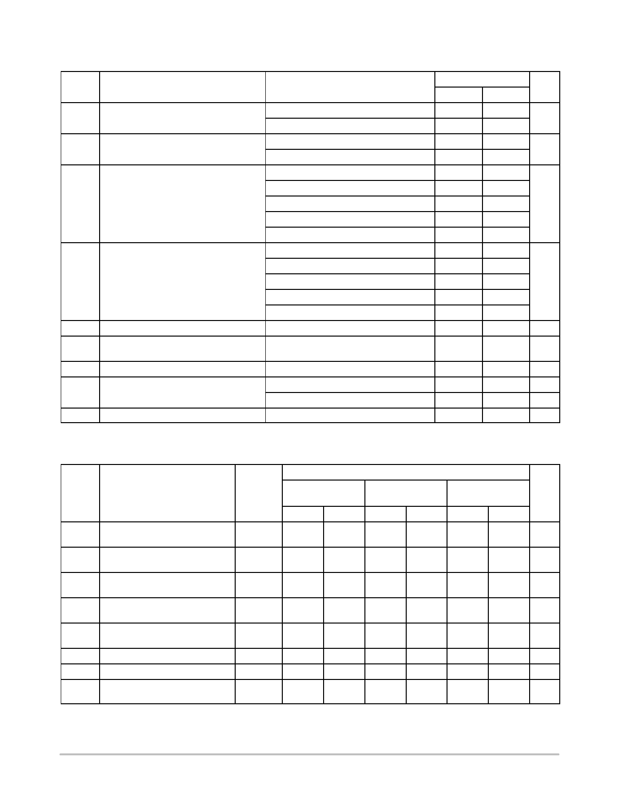
DC ELECTRICAL CHARACTERISTICS
Symbol
Characteristic
Condition
VIH HIGH Level Input Voltage (Note 2)
2.3 V ≤ VCC ≤ 2.7 V
2.7 V ≤ VCC ≤ 3.6 V
VIL LOW Level Input Voltage (Note 2)
2.3 V ≤ VCC ≤ 2.7 V
2.7 V ≤ VCC ≤ 3.6 V
VOH HIGH Level Output Voltage
2.3 V ≤ VCC ≤ 3.6 V; IOL = 100 mA
VCC = 2.3 V; IOH = −8 mA
VCC = 2.7 V; IOH = −12 mA
VCC = 3.0 V; IOH = −18 mA
VCC = 3.0 V; IOH = −24 mA
VOL LOW Level Output Voltage
2.3 V ≤ VCC ≤ 3.6 V; IOL = 100 mA
VCC = 2.3 V; IOL= 8 mA
VCC = 2.7 V; IOL= 12 mA
VCC = 3.0 V; IOL = 16 mA
VCC = 3.0 V; IOL = 24 mA
II
Input Leakage Current
2.3 V ≤ VCC ≤ 3.6 V; 0 V ≤ VI ≤ 5.5 V
IOZ 3−State Output Current
2.3 ≤ VCC ≤ 3.6 V; 0V ≤ VO ≤ 5.5 V;
VI = VIH or V IL
IOFF Power−Off Leakage Current
VCC = 0 V; VI or VO = 5.5 V
ICC Quiescent Supply Current
2.3 ≤ VCC ≤ 3.6 V; VI = GND or VCC
2.3 ≤ VCC ≤ 3.6 V; 3.6 ≤ VI or VO ≤ 5.5 V
DICC Increase in ICC per Input
2.3 ≤ VCC ≤ 3.6 V; VIH = VCC − 0.6 V
2. These values of VI are used to test DC electrical characteristics only.
TA = −40°C to +85°C
Min
Max
Unit
1.7
V
2.0
0.7
V
0.8
VCC − 0.2
V
1.8
2.2
2.4
2.2
0.2
V
0.6
0.4
0.4
0.55
±5.0
mA
±5.0
mA
10
mA
20
mA
±20
mA
500
mA
AC CHARACTERISTICS tR = tF = 2.5 ns; CL = 50 pF; RL = 500 W
VCC = 3.3 V ± 0.3 V
CL = 50 pF
TA = −40°C to +85°C
VCC = 2.7 V
CL = 50 pF
VCC = 2.5 V ± 0.2 V
CL = 30 pF
Symbol
Parameter
Waveform Min
Max
Min
Max
Min
Max Unit
tPLH Propagation Delay
tPHL Dn to On
1
1.5
5.4
1.5
5.9
1.5
6.5
ns
1.5
5.4
1.5
5.9
1.5
6.5
tPLH Propagation Delay
tPHL LE to On
3
1.5
5.5
1.5
6.4
1.5
6.6
ns
1.5
5.5
1.5
6.4
1.5
6.6
tPZH Output Enable Time to
tPZL High and Low Level
2
1.5
6.1
1.5
6.5
1.5
7.9
ns
1.5
6.1
1.5
6.5
1.5
7.9
tPHZ Output Disable Time From
tPLZ High and Low Level
2
1.5
6.0
1.5
6.3
1.5
7.2
ns
1.5
6.0
1.5
6.3
1.5
7.2
ts
Setup Time, HIGH or LOW Dn to
3
2.5
2.5
3.0
ns
LE
th
Hold Time, HIGH or LOW Dn to LE
3
1.5
1.5
2.0
ns
tw
LE Pulse Width, HIGH
3
3.0
3.0
3.5
ns
tOSHL Output−to−Output Skew
1.0
ns
tOSLH (Note 3)
1.0
3. Skew is defined as the absolute value of the difference between the actual propagation delay for any two separate outputs of the same device.
The specification applies to any outputs switching in the same direction, either HIGH−to−LOW (tOSHL) or LOW−to−HIGH (tOSLH); parameter
guaranteed by design.
http://onsemi.com
4
Share Link: 