MC74VHCT240AMELG Ver la hoja de datos (PDF) - ON Semiconductor
Número de pieza
componentes Descripción
Lista de partido
MC74VHCT240AMELG Datasheet PDF : 7 Pages
| |||
MC74VHCT240A
A1 2
A2 4
18 YA1
16 YA2
OEA 1
A1 2
YB4 3
20 VCC
19 OEB
18 YA1
A3 6
DATA
INPUTS
A4 8
B1 11
14 YA3
12 YA4
9 YB1
INVERTING
OUTPUTS
A2 4
YB3 5
A3 6
YB2 7
A4 8
17 B4
16 YA2
15 B3
14 YA3
13 B2
B2 13
B3 15
B4 17
7 YB2
5 YB3
3 YB4
YB1 9
GND 10
12 YA4
11 B1
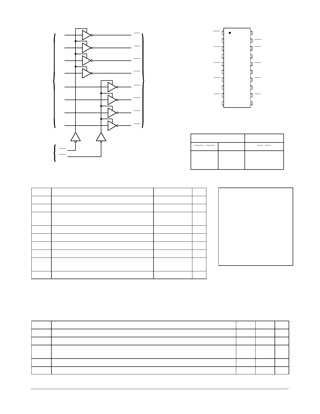
Figure 2. Pin Assignment
FUNCTION TABLE
INPUTS
OUTPUTS
OUTPUT OEA 1
ENABLES OEB 19
Figure 1. Logic Diagram
OEA, OEB
L
L
H
A, B
L
H
X
YA, YB
H
L
Z
ÎÎÎÎÎÎÎÎÎÎÎÎÎÎÎÎÎÎÎÎÎÎÎ MAXIMUM RATINGS
ÎÎÎÎÎÎÎÎÎÎÎÎÎÎÎÎÎÎÎÎÎÎÎ Symbol
Parameter
Value
Unit
ÎÎÎÎÎÎÎÎÎÎÎÎÎÎÎÎÎÎÎÎÎÎÎ VCC DC Supply Voltage
– 0.5 to + 7.0
V
ÎÎÎÎÎÎÎÎÎÎÎÎÎÎÎÎÎÎÎÎÎÎÎ Vin DC Input Voltage
– 0.5 to + 7.0
V
ÎÎÎÎÎÎÎÎÎÎÎÎÎÎÎÎÎÎÎÎÎÎÎ Vout DC Output Voltage
Output in 3−State – 0.5 to + 7.0
V
High or Low State – 0.5 to VCC + 0.5
ÎÎÎÎÎÎÎÎÎÎÎÎÎÎÎÎÎÎÎÎÎÎÎ IIK Input Diode Current
− 20
mA
ÎÎÎÎÎÎÎÎÎÎÎÎÎÎÎÎÎÎÎÎÎÎÎ IOK Output Diode Current (VOUT < GND; VOUT > VCC)
± 20
mA
ÎÎÎÎÎÎÎÎÎÎÎÎÎÎÎÎÎÎÎÎÎÎÎ Iout DC Output Current, per Pin
± 25
mA
ÎÎÎÎÎÎÎÎÎÎÎÎÎÎÎÎÎÎÎÎÎÎÎ ICC DC Supply Current, VCC and GND Pins
± 75
mA
ÎÎÎÎÎÎÎÎÎÎÎÎÎÎÎÎÎÎÎÎÎÎÎ PD Power Dissipation in Still Air,
SOIC Packages†
500
mW
ÎÎÎÎÎÎÎÎÎÎÎÎÎÎÎÎÎÎÎÎÎÎÎ TSSOP Package†
450
ÎÎÎÎÎÎÎÎÎÎÎÎÎÎÎÎÎÎÎÎÎÎÎÎÎÎÎÎÎÎÎÎÎÎÎÎÎÎÎÎÎÎÎÎÎÎ Tstg StorageTemperature
– 65 to + 150
_C
Maximum ratings are those values beyond which device damage can occur. Maximum ratings
This device contains protection
circuitry to guard against damage
due to high static voltages or electric
fields. However, precautions must
be taken to avoid applications of any
voltage higher than maximum rated
voltages to this high−impedance cir-
cuit. For proper operation, Vin and
Vout should be constrained to the
range GND v (Vin or Vout) v VCC.
Unused inputs must always be
tied to an appropriate logic voltage
level (e.g., either GND or VCC).
Unused outputs must be left open.
applied to the device are individual stress limit values (not normal operating conditions) and are
not valid simultaneously. If these limits are exceeded, device functional operation is not implied,
damage may occur and reliability may be affected.
†Derating − SOIC Packages: – 7 mW/_C from 65_ to 125_C
TSSOP Package: − 6.1 mW/_C from 65_ to 125_C
RECOMMENDED OPERATING CONDITIONS
ÎÎÎÎÎÎÎÎÎÎÎÎÎÎÎÎÎÎÎÎÎÎÎÎÎÎÎÎÎÎÎÎÎ Symbol
Parameter
ÎÎÎÎÎÎÎÎÎÎÎÎÎÎÎÎÎÎÎÎÎÎÎÎÎÎÎÎÎÎÎÎÎ VCC DCSupplyVoltage
ÎÎÎÎÎÎÎÎÎÎÎÎÎÎÎÎÎÎÎÎÎÎÎÎÎÎÎÎÎÎÎÎÎ Vin DCInputVoltage
ÎÎÎÎÎÎÎÎÎÎÎÎÎÎÎÎÎÎÎÎÎÎÎÎÎÎÎÎÎÎÎÎÎÎÎÎÎÎÎÎÎÎÎÎÎÎÎÎÎÎÎÎÎÎÎÎÎÎÎÎÎÎÎÎÎÎ Vout DCOutputVoltage
Output in 3−State
High or Low State
ÎÎÎÎÎÎÎÎÎÎÎÎÎÎÎÎÎÎÎÎÎÎÎÎÎÎÎÎÎÎÎÎÎ TA Operating Temperature
ÎÎÎÎÎÎÎÎÎÎÎÎÎÎÎÎÎÎÎÎÎÎÎÎÎÎÎÎÎÎÎÎÎÎÎÎÎÎÎÎÎÎÎÎÎÎÎÎÎÎÎÎÎÎÎÎÎÎÎÎÎÎÎÎÎÎ tr,tf InputRiseandFallTime
VCC =5.0V ±0.5V
Min
Max Unit
4.5
5.5
V
0
5.5
V
0
5.5
V
0
VCC
− 40
+ 85 _C
0
20 ns/V
http://onsemi.com
2
Share Link: 