OZ6812 Ver la hoja de datos (PDF) - Unspecified
Número de pieza
componentes Descripción
Lista de partido
OZ6812 Datasheet PDF : 13 Pages
| |||
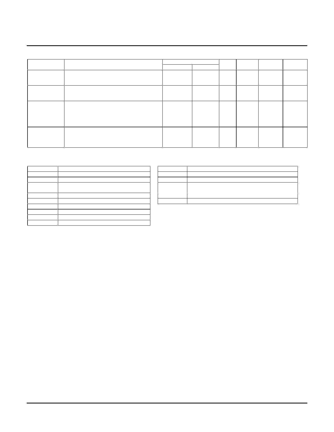
Power, Ground, and Reserved Pins
OZ6812
Pin Name
Aux_VCC
CORE_VCC
PCI_VCC
GND
Description
Auxiliary VCC: This pin is connected to the
system’s 3.3/5V power supply. For the device
to 5V tolerant, connect to +5V power.
CORE_VCC: This pin provides power to the
core circuitry of the OZ6812. It must be
connected to a 3.3V power supply.
PCI Bus VCC: These pins can be connected to
either a 3.3V or5V power supply. The PCI bus
interface will operate at the voltage applied to
these pins, independent of the voltage applied
to other OZ6812 pin groups.
System Ground
Pin Number
LQFP
BGA
63
M9
14, 66, 86,
102, 122,
138
18, 30, 44,
50
F4, M10,
H10, D12,
D8, B4
G3, K2,
M4, K6
6, 22, 42,
58, 78, 94,
114, 130
D3, H1,
L4, N8,
K11, F13,
C10, A6
Input
-
-
-
-
Type
PWR
PWR
PWR
GND
Power
Rail
-
-
-
-
Drive
-
-
-
-
Legend
I/O Type
I
I-PU
I-PU Schmitt
O
OD
TO
TO-PU
OD-PU
PWR
Description
Input Pin
Input pin with internal pull-up
Input pin with internal pull-up and Schmitt
trigger
Output
Open-drain
Tri-state output
Tri-state output with internal pull-up
Open-drain output with internal pull-up
Power pin
Power Rail
1
2
3
Source of Output’s Power
AUX_VCC: outputs powered from AUX_VCC
SOCKET_VCC: outputs powered from the socket
PCI_VCC: outputs powered from PCI bus power
supply
4
CORE_VCC: outputs powered from the CORE_VCC
OZ6812-SF-1.5
Page 11
Share Link: 