PI74ALVCH32245 Ver la hoja de datos (PDF) - Pericom Semiconductor
Número de pieza
componentes Descripción
Lista de partido
PI74ALVCH32245 Datasheet PDF : 7 Pages
| |||
PI74ALVCH32245
3.3V, 32-Bit Bidirectional Tranceiver
with 3-State Outputs 1122334455667788990011223344556677889900112233445566778899001122112233445566778899001122334455667788990011223344556677889900112211223344556677889900112233445566778899001122334455667788990011221122334455667788990011223344556677889900112233445566778899001122112233445566778899001122
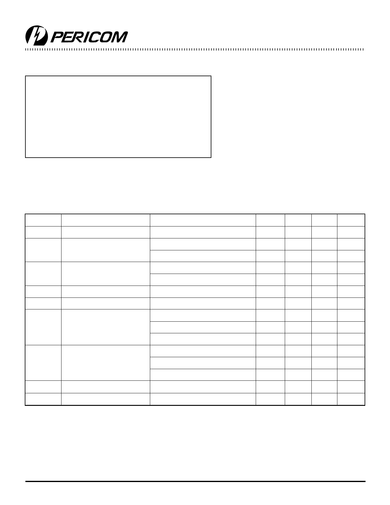
Maximum Ratings
(Above which the useful life may be impaired. For user guidelines, not tested.)
Supply Voltage Range,VCC ............................................................... 0.5V to 4.6V
Input Voltage Range, VI: Except I/O ports (1) .............................. 0.5V to 4.6V
I/O ports (1,2) ........................... 0.5V to VCC + 0.5V
Output Voltage Range, VO (1,2) ............................................ 0.5V to VCC +0.5V
Input Clamp Current, IIK (VI <0) ........................................................ 50mA
Output Clamp Current, IOK (VO <0) .................................................. 50mA
Continuous Output Current, IO ................................................................... ±50mA
Continuous Current through each VCC or GND ............................... ±100mA
Package Thermal Impedance, θJA(3) ............................................................. 40ºC/W
Storage Temperature Range, TSTG ............................................... 65ºC to 150ºC
Note:
Stresses greater than those listed under MAXIMUM
RATINGS may cause permanent damage to the device.
This is a stress rating only and functional operation of the
device at these or any other conditions above those indi-
cated in the operational sections of this specification is not
implied. Exposure to absolute maximum rating conditions
for extended periods may affect reliability.
Note:
1. The input negative voltage and output voltage ratings may be exceeded
if the input and output current ratings are observed.
2. This value is limited to 4.6V maximum.
3. The package thermal impedance is calculated in accordance with JESD 51.
Recommended Operating Conditions(1)
Parameters
Description
Test Conditions
Min.
Typ. Max. Units
VCC
Supply Voltage
2.3
VIH
Input HIGH Voltage
VCC = 2.3V to 2.7V
1.7
VCC = 2.7V to 3.6V
2.0
VIL
Input LOW Voltage
VCC = 2.3V to 2.7V
VCC = 2.7V to 3.6V
VIN
Input Voltage
0
VOUT
Output Voltage
0
Output
IOH
HIGH
Current
VCC = 2.3V
VCC = 2.7V
VCC = 3.0V
Output
IOL
LOW
Current
VCC = 2.3V
VCC = 2.7V
VCC = 3.0V
∆t/∆V Input Transition Rise or Fall Rate
0
3.6
V
0.7
0.8
VCC
VCC
12
mA
12
24
12
12
24
10
ns/V
TA
Operating Free-Air Temperature
40
Note 1: All unused inputs must be held at VCC or GND to ensure proper device operation
85
°C
3
PS8437 08/24/01
Share Link: 