V62C2164096L-85T Ver la hoja de datos (PDF) - Mosel Vitelic Corporation
Número de pieza
componentes Descripción
Lista de partido
V62C2164096L-85T Datasheet PDF : 10 Pages
| |||
MOSEL VITELIC
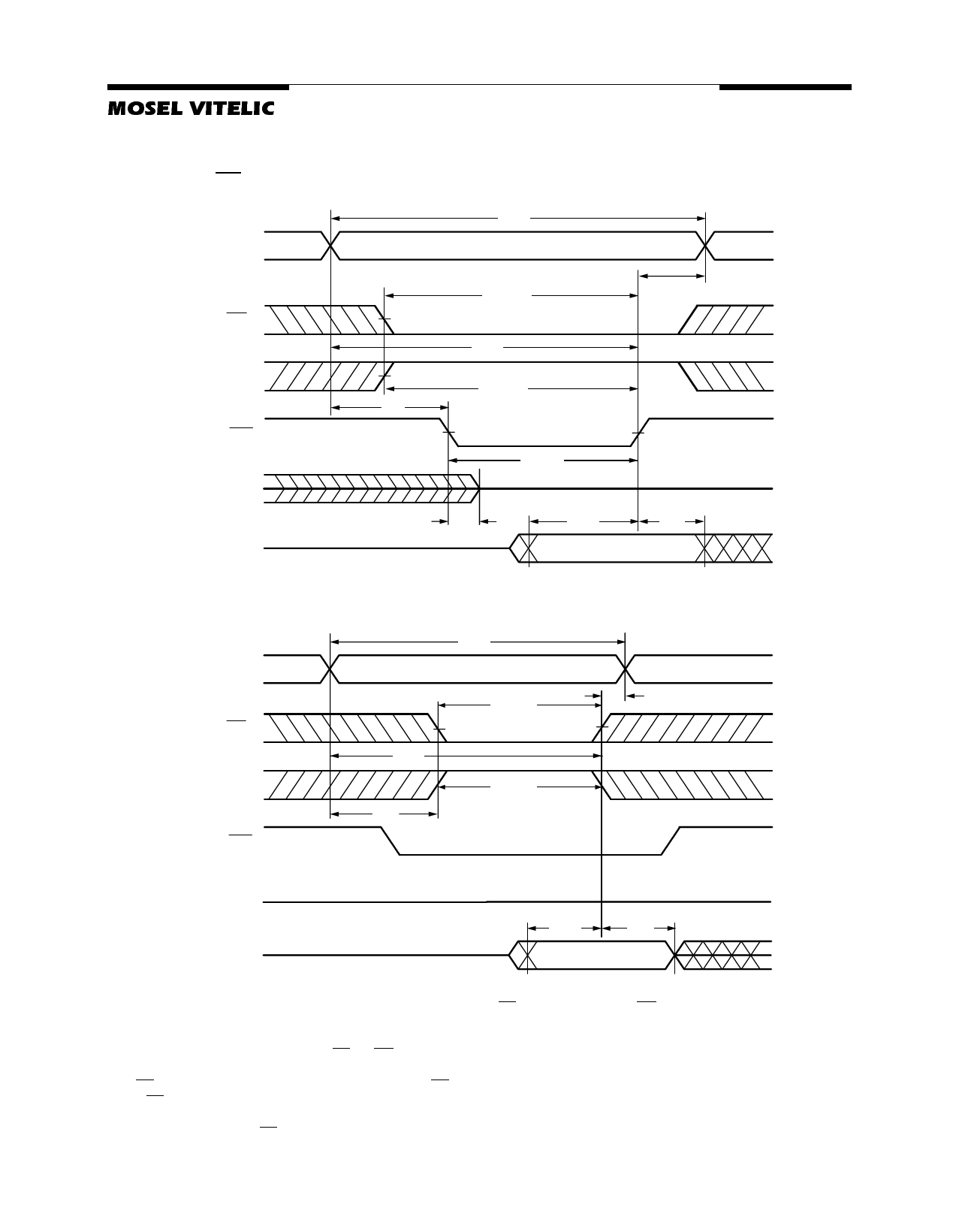
Switching Waveforms (Write Cycle)
Write Cycle 1 (WE Controlled)(4, 7)
ADDRESS
CE1
CE2
WE
OUTPUT
INPUT
tAS
tWHZ
tWC
tCW(6)
tAW
tCW(6)
tWP(1)
tDW
V62C2164096
tWR(2)
tDH
Write Cycle 2 (CE Controlled)(4, 7)
ADDRESS
CE1
CE2
WE
tAW
tAS
tWC
tCW(6)
(4)
tCW(6)
tWR(2)
OUTPUT
INPUT
High-Z
tDW
tDH
(5)
NOTES:
1. The internal write time of the memory is defined by the overlap of CE1 and CE2 active and WE low. All signals must be active to
initiate and any one signal can terminate a write by going inactive. The data input setup and hold timing should be referenced to
the second transition edge of the signal that terminates the write.
2. tWR is measured from the earlier of CE1 or WE going high, or CE2 going LOW at the end of the write cycle.
3. During this period, I/O pins are in the output state so that the input signals of opposite phase to the outputs must not be applied.
4. OE = VIL or VIH. However it is recommended to keep OE at VIH during write cycle to avoid bus contention.
5. If CE1 is LOW and CE2 is HIGH during this period, I/O pins are in the output state. Then the data input signals of opposite phase
to the outputs must not be applied to them.
6. tCW is measured from CE1 going low or CE2 going HIGH to the end of write.
7. CE2 is available on BGA package only.
V62C2164096 Rev. 1.0 November 2001
8
Share Link: 