IRF5N3710 Ver la hoja de datos (PDF) - International Rectifier
Número de pieza
componentes Descripción
Lista de partido
IRF5N3710 Datasheet PDF : 7 Pages
| |||
IRF5N3710
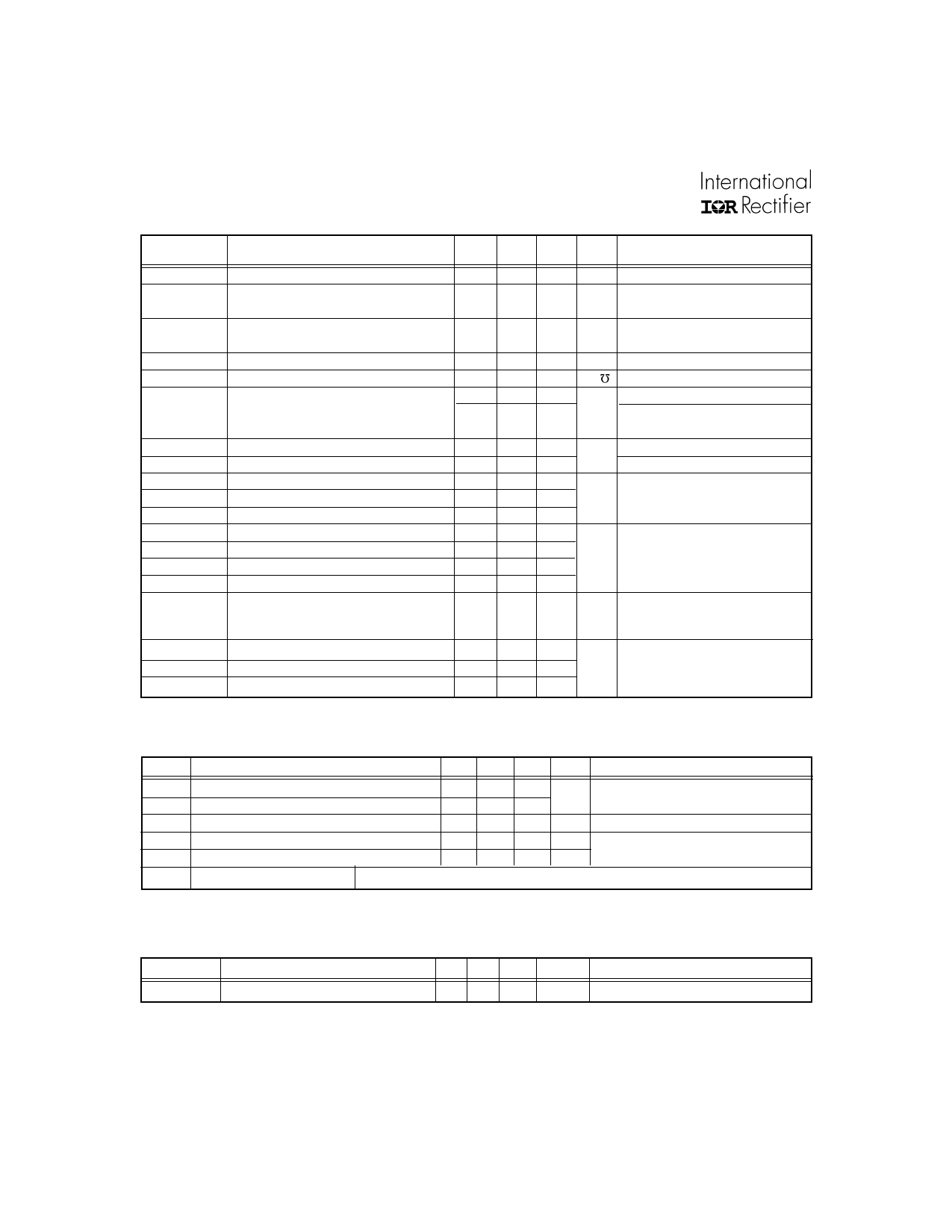
Electrical Characteristics @ Tj = 25°C (Unless Otherwise Specified)
Parameter
Min Typ Max Units
Test Conditions
BVDSS
Drain-to-Source Breakdown Voltage 100 — — V
VGS = 0V, ID = 250µA
∆BVDSS/∆TJ Temperature Coefficient of Breakdown — 0.104 — V/°C Reference to 25°C, ID = 1.0mA
Voltage
RDS(on)
Static Drain-to-Source On-State
Resistance
— — 0.028 Ω
VGS = 10V, ID = 28A ➃
VGS(th)
gfs
IDSS
IGSS
IGSS
Qg
Qgs
Qgd
td(on)
tr
td(off)
tf
LS + LD
Gate Threshold Voltage
Forward Transconductance
Zero Gate Voltage Drain Current
Gate-to-Source Leakage Forward
Gate-to-Source Leakage Reverse
Total Gate Charge
Gate-to-Source Charge
Gate-to-Drain (‘Miller’) Charge
Turn-On Delay Time
Rise Time
Turn-Off Delay Time
Fall Time
Total Inductance
2.0 — 4.0 V
20 — — S ( )
—
—
—
—
25
250
µA
— — 100
—
— -100 nA
— — 200
— — 28 nC
— — 94
VDS = VGS, ID = 250µA
VDS =15V, IDS = 28A ➃
VDS = 100V ,VGS=0V
VDS = 80V,
VGS = 0V, TJ =125°C
VGS =-20V
VGS = -20V
VGS =10V, ID = 28A
VDS = 80V
— — 25
— — 86
—
— 75
ns
VDD = 50V, ID = 28A,
VGS = 10V, RG = 2.5Ω
— — 54
— 4.0 — nH
Measured from the center of
drain pad to center of source pad
Ciss
Coss
Crss
Input Capacitance
Output Capacitance
Reverse Transfer Capacitance
— 2920 —
— 700 — pF
— 340 —
VGS = 0V, VDS = 25V
f = 1.0MHz
Source-Drain Diode Ratings and Characteristics
Parameter
Min Typ Max Units
Test Conditions
IS
Continuous Source Current (Body Diode) — — 45
A
ISM Pulse Source Current (Body Diode) ➀
— — 180
VSD Diode Forward Voltage
— — 1.3 V
trr Reverse Recovery Time
— — 280 ns
QRR Reverse Recovery Charge
— — 2.0 µC
Tj = 25°C, IS = 28A, VGS = 0V ➃
Tj = 25°C, IF = 28A, di/dt ≤ 100A/µs
VDD ≤ 50V ➃
ton Forward Turn-On Time
Intrinsic turn-on time is negligible. Turn-on speed is substantially controlled by LS + LD.
Thermal Resistance
Parameter
RthJC
Junction-to-Case
Min Typ Max Units
— — 1.0 °C/W
Test Conditions
Note: Corresponding Spice and Saber models are available on the G&S Website.
For footnotes refer to the last page
2
www.irf.com
Share Link: 