IRF7604 Ver la hoja de datos (PDF) - International Rectifier
Número de pieza
componentes Descripción
Lista de partido
IRF7604 Datasheet PDF : 8 Pages
| |||
IRF7604
Electrical Characteristics @ TJ = 25°C (unless otherwise specified)
Parameter
Min. Typ. Max. Units
Conditions
V(BR)DSS Drain-to-Source Breakdown Voltage
-20 ––– ––– V VGS = 0V, ID = -250µA
∆V(BR)DSS/∆TJ Breakdown Voltage Temp. Coefficient ––– -0.022 ––– V/°C Reference to 25°C, ID = -1mA
RDS(ON)
Static Drain-to-Source On-Resistance
––– ––– 0.090
––– ––– 0.13 Ω
VGS = -4.5V, ID = -2.4A
VGS = -2.7V, ID = -1.2A
VGS(th)
Gate Threshold Voltage
-0.70 ––– ––– V VDS = VGS, ID = -250µA
gfs
Forward Transconductance
2.6 ––– ––– S VDS = -10V, ID = -1.2A
IDSS
Drain-to-Source Leakage Current
––– ––– -1.0
––– ––– -25
µA VDS = -16V, VGS = 0V
VDS = -16V, VGS = 0V, TJ = 125°C
IGSS
Gate-to-Source Forward Leakage
Gate-to-Source Reverse Leakage
––– ––– -100 nA VGS = -12V
––– ––– 100
VGS = 12V
Qg
Total Gate Charge
––– 13 20
ID = -2.4A
Qgs
Gate-to-Source Charge
––– 2.6 3.9 nC VDS = -16V
Qgd
Gate-to-Drain ("Miller") Charge
––– 5.6 9.0
VGS = -4.5V, See Fig. 6 and 9
td(on)
Turn-On Delay Time
––– 17 –––
VDD = -10V
tr
td(off)
Rise Time
Turn-Off Delay Time
––– 53 –––
––– 31 –––
ns
ID = -2.4A
RG = 6.0Ω
tf
Fall Time
––– 38 –––
RD = 4.0Ω, See Fig. 10
Ciss
Input Capacitance
––– 590 –––
VGS = 0V
Coss
Output Capacitance
––– 330 ––– pF VDS = -15V
Crss
Reverse Transfer Capacitance
––– 170 –––
ƒ = 1.0MHz, See Fig. 5
Source-Drain Ratings and Characteristics
Parameter
IS
Continuous Source Current
(Body Diode)
ISM
Pulsed Source Current
(Body Diode)
VSD
Diode Forward Voltage
trr
Reverse Recovery Time
Qrr
Reverse Recovery Charge
Min. Typ. Max. Units
Conditions
––– ––– -1.8
––– ––– -19
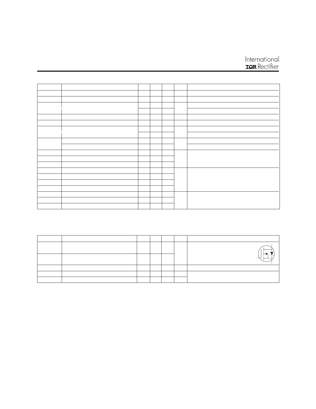
MOSFET symbol
A showing the
integral reverse
p-n junction diode.
D
G
S
––– ––– -1.2 V TJ = 25°C, IS = -2.4A, VGS = 0V
––– 41 62 ns TJ = 25°C, IF = -2.4A
––– 38 57 nC di/dt = 100A/µs
Notes:
Repetitive rating; pulse width limited by
max. junction temperature. ( See fig. 11 )
Pulse width ≤ 300µs; duty cycle ≤ 2%.
ISD ≤ -2.4A, di/dt ≤ -96A/µs, VDD ≤ V(BR)DSS,
TJ ≤ 150°C
Surface mounted on FR-4 board, t ≤ 10sec.
Share Link: 