IRFS42N20D Ver la hoja de datos (PDF) - International Rectifier
Número de pieza
componentes Descripción
Lista de partido
IRFS42N20D Datasheet PDF : 6 Pages
| |||
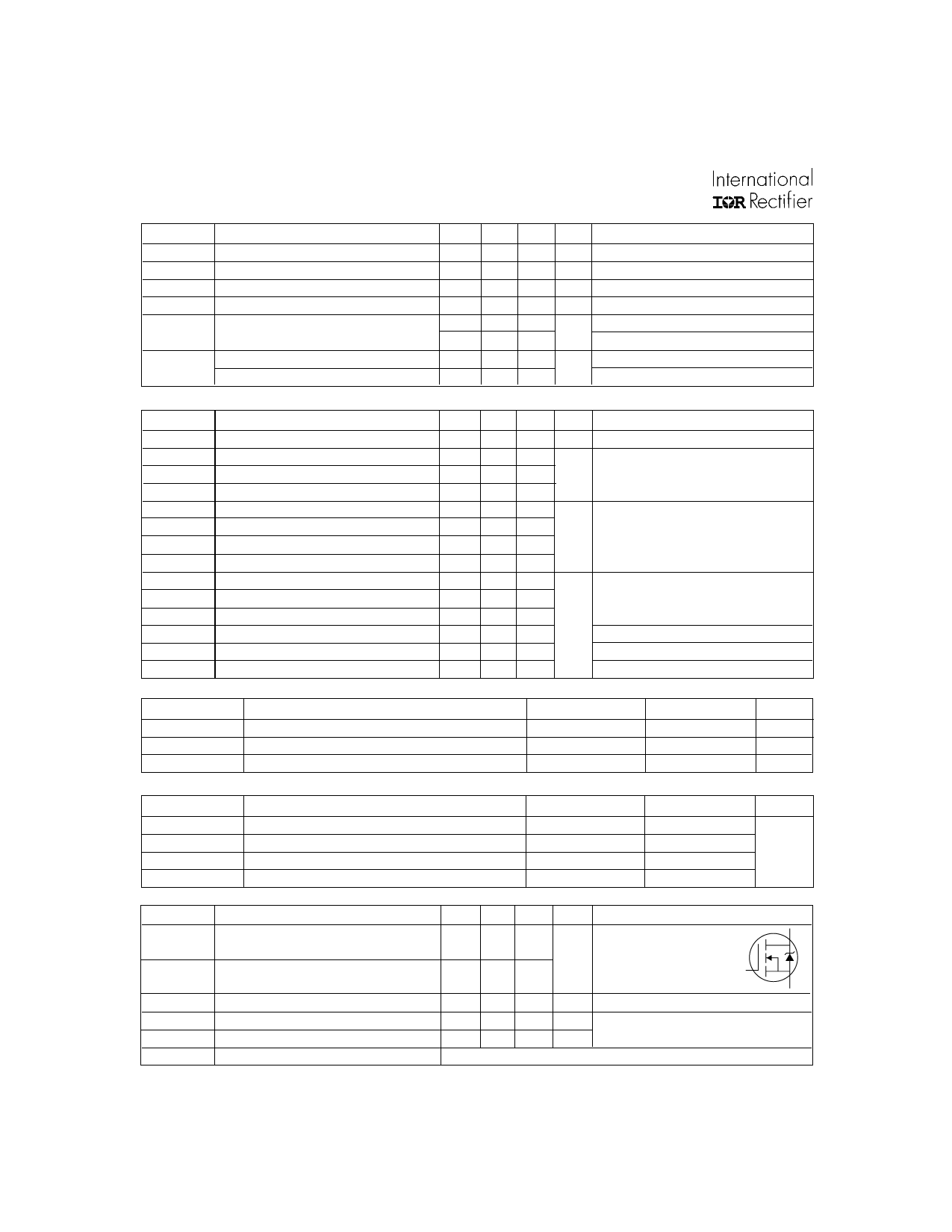
IRFB/IRFS/IRFSL42N20D
PROVISIONAL
Static @ TJ = 25°C (unless otherwise specified)
Parameter
V(BR)DSS Drain-to-Source Breakdown Voltage
∆V(BR)DSS/∆TJ Breakdown Voltage Temp. Coefficient
RDS(on)
Static Drain-to-Source On-Resistance
VGS(th)
Gate Threshold Voltage
IDSS
Drain-to-Source Leakage Current
Gate-to-Source Forward Leakage
IGSS
Gate-to-Source Reverse Leakage
Min.
200
–––
–––
3.0
–––
–––
–––
–––
Typ. Max.
––– –––
TBD –––
––– 0.055
––– 5.5
––– 25
––– 250
––– 100
––– -100
Units
V
V/°C
Ω
V
µA
nA
Conditions
VGS = 0V, ID = 250µA
Reference to 25°C, ID = 1mA
VGS = 10V, ID = 25.5A
VDS = VGS, ID = 250µA
VDS = 200V, VGS = 0V
VDS = 160V, VGS = 0V, TJ = 150°C
VGS = 30V
VGS = -30V
Dynamic @ TJ = 25°C (unless otherwise specified)
Parameter
Min. Typ. Max.
gfs
Forward Transconductance
TBD ––– –––
Qg
Total Gate Charge
––– 103 –––
Qgs
Gate-to-Source Charge
––– 26 –––
Qgd
Gate-to-Drain ("Miller") Charge
––– 48 –––
td(on)
Turn-On Delay Time
––– TBD –––
tr
Rise Time
––– TBD –––
td(off)
Turn-Off Delay Time
––– TBD –––
tf
Fall Time
––– TBD –––
Ciss
Input Capacitance
––– 3470 –––
Coss
Output Capacitance
––– 560 –––
Crss
Reverse Transfer Capacitance
––– 120 –––
Coss
Output Capacitance
––– TBD –––
Coss
Output Capacitance
––– TBD –––
Coss eff. Effective Output Capacitance
Avalanche Characteristics
––– TBD –––
Units
S
nC
ns
pF
Conditions
VDS = 25V, ID = 25.5A
ID = 25.5A
VDS = 160V
VGS = 10V
VDD = 100V
ID = 25.5A
RG = TBDΩ
VGS = 10V
VGS = 0V
VDS = 25V
ƒ = 1.0MHz
VGS = 0V, VDS = 1.0V, ƒ = 1.0MHz
VGS = 0V, VDS = 160V, ƒ = 1.0MHz
VGS = 0V, VDS = 0V to 160V
Parameter
EAS
Single Pulse Avalanche Energy
IAR
Avalanche Current
EAR
Repetitive Avalanche Energy
Thermal Resistance
Typ.
–––
–––
–––
Max.
TBD
25.5
30
Units
mJ
A
mJ
Parameter
Typ.
Max.
Units
RθJC
Junction-to-Case
RθCS
Case-to-Sink, Flat, Greased Surface
RθJA
Junction-to-Ambient
RθJA
Junction-to-Ambient
Diode Characteristics
–––
0.5
0.50
–––
°C/W
–––
62
–––
40
Parameter
Min. Typ. Max. Units
Conditions
IS
Continuous Source Current
(Body Diode)
ISM
Pulsed Source Current
(Body Diode)
MOSFET symbol
D
––– ––– 42.6 A showing the
––– ––– 170
integral reverse
G
p-n junction diode.
S
VSD
Diode Forward Voltage
trr
Reverse Recovery Time
Qrr
Reverse RecoveryCharge
ton
Forward Turn-On Time
2
––– ––– 1.3 V TJ = 25°C, IS = 25.5A, VGS = 0V
––– TBD TBD ns TJ = 25°C, IF = 25.5A
––– 2.4 3.6 µC di/dt = 100A/µs
Intrinsic turn-on time is negligible (turn-on is dominated by LS+LD)
www.irf.com
Share Link: 