IRF3706L Ver la hoja de datos (PDF) - International Rectifier
Número de pieza
componentes Descripción
Lista de partido
IRF3706L Datasheet PDF : 11 Pages
| |||
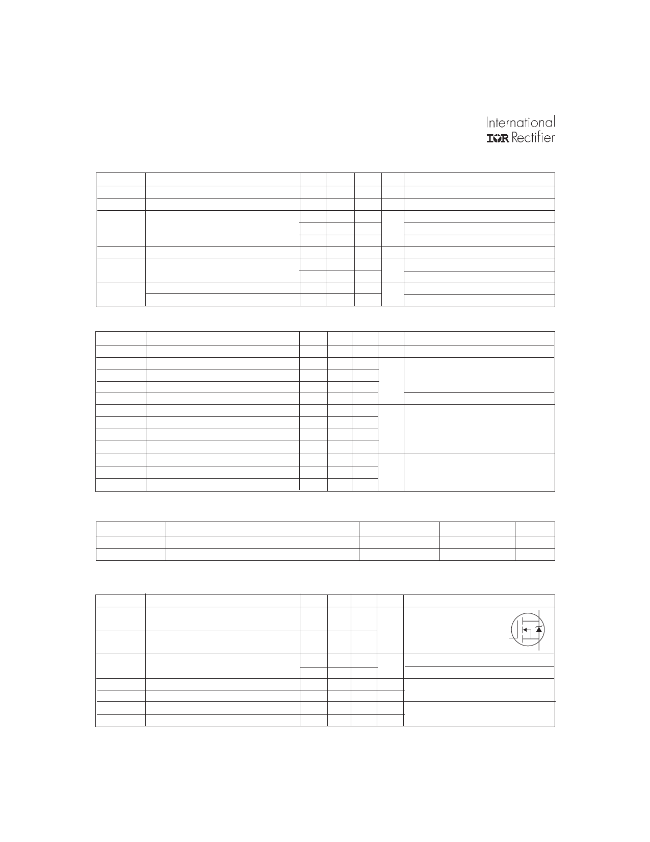
IRF3706/3706S/3706L
Static @ TJ = 25°C (unless otherwise specified)
Parameter
Min. Typ. Max. Units
Conditions
V(BR)DSS Drain-to-Source Breakdown Voltage 20 ––– ––– V VGS = 0V, ID = 250µA
∆V(BR)DSS/∆TJ Breakdown Voltage Temp. Coefficient –––
–––
RDS(on)
Static Drain-to-Source On-Resistance –––
–––
VGS(th)
Gate Threshold Voltage
0.6
–––
IDSS
Drain-to-Source Leakage Current
–––
Gate-to-Source Forward Leakage
–––
IGSS
Gate-to-Source Reverse Leakage –––
0.021
6.0
7.3
11
–––
–––
–––
–––
–––
–––
8.5
10.5
22
2.0
20
100
200
-200
V/°C Reference to 25°C, ID = 1mA
VGS = 10V, ID = 36A
mΩ VGS = 4.5V, ID = 28A
VGS = 2.8V, ID = 18A
V VDS = VGS, ID = 250µA
µA VDS = 16V, VGS = 0V
VDS = 16V, VGS = 0V, TJ = 125°C
nA VGS = 12V
VGS = -12V
Dynamic @ TJ = 25°C (unless otherwise specified)
Symbol
Parameter
Min. Typ. Max. Units
Conditions
gfs
Forward Transconductance
53 ––– ––– S VDS = 16V, ID = 57A
Qg
Total Gate Charge
Qgs
Gate-to-Source Charge
––– 23 35
––– 8.0 12
ID = 28A
nC VDS = 10V
Qgd
Qoss
Gate-to-Drain ("Miller") Charge
Output Gate Charge
––– 5.5 8.3
––– 16 24
VGS = 4.5V
VGS = 0V, VDS = 10V
td(on)
tr
td(off)
tf
Turn-On Delay Time
Rise Time
Turn-Off Delay Time
Fall Time
––– 6.8 –––
VDD = 10V
––– 87 ––– ns ID = 28A
––– 17 –––
RG = 1.8Ω
––– 4.8 –––
VGS = 4.5V
Ciss
Input Capacitance
––– 2410 –––
VGS = 0V
Coss
Output Capacitance
––– 1070 –––
VDS = 10V
Crss
Reverse Transfer Capacitance
––– 140 ––– pF ƒ = 1.0MHz
Avalanche Characteristics
Symbol
EAS
IAR
Parameter
Single Pulse Avalanche Energy
Avalanche Current
Typ.
–––
–––
Max.
220
28
Units
mJ
A
Diode Characteristics
Symbol
IS
ISM
Parameter
Continuous Source Current
(Body Diode)
Pulsed Source Current
(Body Diode)
VSD
Diode Forward Voltage
trr
Reverse Recovery Time
Qrr
Reverse Recovery Charge
trr
Reverse Recovery Time
Qrr
Reverse Recovery Charge
2
Min. Typ. Max. Units
Conditions
MOSFET symbol
D
––– ––– 77
A
showing the
integral reverse
G
––– ––– 280
p-n junction diode.
S
––– 0.88 1.3 V TJ = 25°C, IS = 36A, VGS = 0V
––– 0.82 –––
TJ = 125°C, IS = 36A, VGS = 0V
––– 45 68
––– 65 98
ns TJ = 25°C, IF = 36A, VR=20V
nC di/dt = 100A/µs
––– 49 74 ns TJ = 125°C, IF = 36A, VR=20V
––– 78 120 nC di/dt = 100A/µs
www.irf.com
Share Link: 