IRFP17N50LS Ver la hoja de datos (PDF) - International Rectifier
Número de pieza
componentes Descripción
Lista de partido
IRFP17N50LS Datasheet PDF : 8 Pages
| |||
PD - 94351
IRFP17N50LS
Applications
SMPS MOSFET HEXFET® Power MOSFET
l Switch Mode Power Supply (SMPS)
l Uninterruptible Power Supply
VDSS RDS(on) typ.
Trr
ID
l High Speed Power Switching
500V
0.28Ω
170ns 16A
l ZVS and High Frequency Circuit
l PWM Inverters
Benefits
l Low Gate Charge Qg results in Simple Drive Requirement
l Improved Gate, Avalanche and Dynamic dv/dt Ruggedness
l Fully Characterized Capacitance and Avalanche Voltage
and Current
l Low Trr and Soft Diode Recovery
l High Performance Optimised Anti-parallel Diode
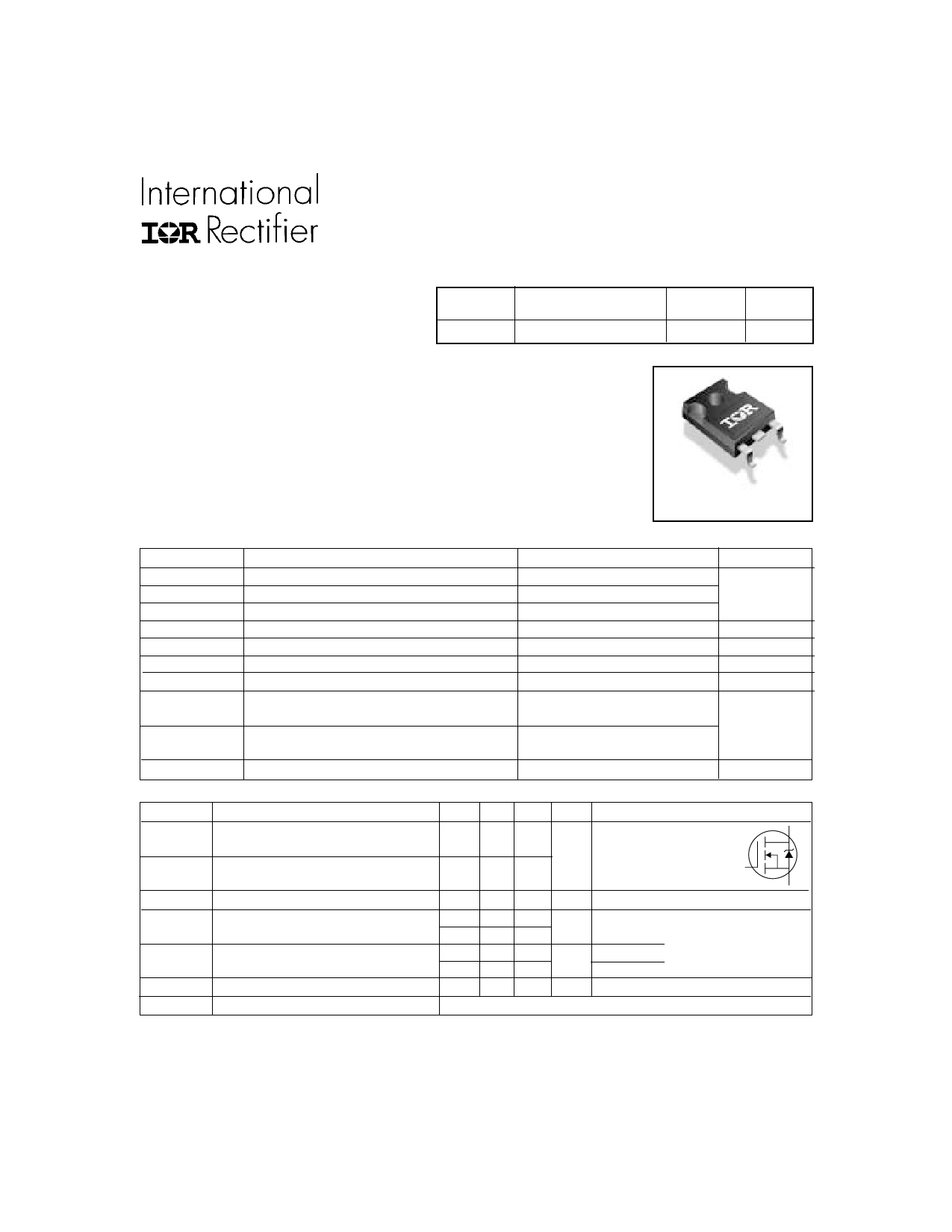
SMD-247
Absolute Maximum Ratings
ID @ TC = 25°C
ID @ TC = 100°C
IDM
PD @TC = 25°C
VGS
dv/dt
TJ
TSTG
Parameter
Continuous Drain Current, VGS @ 10V
Continuous Drain Current, VGS @ 10V
Pulsed Drain Current
Power Dissipation
Linear Derating Factor
Gate-to-Source Voltage
Peak Diode Recovery dv/dt
Operating Junction and
Storage Temperature Range
Soldering Temperature, for 10 seconds
(1.6mm from case )
Max.
16
11
64
220
1.8
± 30
13
-55 to + 150
300
Units
A
W
W/°C
V
V/ns
°C
Mounting Torque, 6-32 or M3 screw
10
lbft.in(N.m)
Diode Characteristics
Symbol
IS
ISM
VSD
trr
Qrr
IRRM
ton
Parameter
Continuous Source Current
(Body Diode)
Pulsed Source Current
(Body Diode)
Diode Forward Voltage
Reverse Recovery Time
Reverse Recovery Charge
Reverse Recovery Current
Forward Turn-On Time
Min. Typ. Max. Units
Conditions
16
MOSFET symbol
D
––– –––
A showing the
64
integral reverse
G
––– –––
p-n junction diode.
S
––– ––– 1.5 V TJ = 25°C, IS = 16A, VGS = 0V
––– 170 250
––– 220 330
ns
TJ = 25°C
TJ = 125°C
IF = 16A
di/dt = 100A/µs
––– 470 710 nC TJ = 25°C
––– 810 1210
TJ = 125°C
––– 7.3 11 A
Intrinsic turn-on time is negligible (turn-on is dominated by LS+LD)
Typical SMPS Topologies
l Bridge Converters
l All Zero Voltage Switching
www.irf.com
1
11/28/01
Share Link: 