IRF3205L Ver la hoja de datos (PDF) - International Rectifier
Número de pieza
componentes Descripción
Lista de partido
IRF3205L Datasheet PDF : 10 Pages
| |||
IRF3205S/L
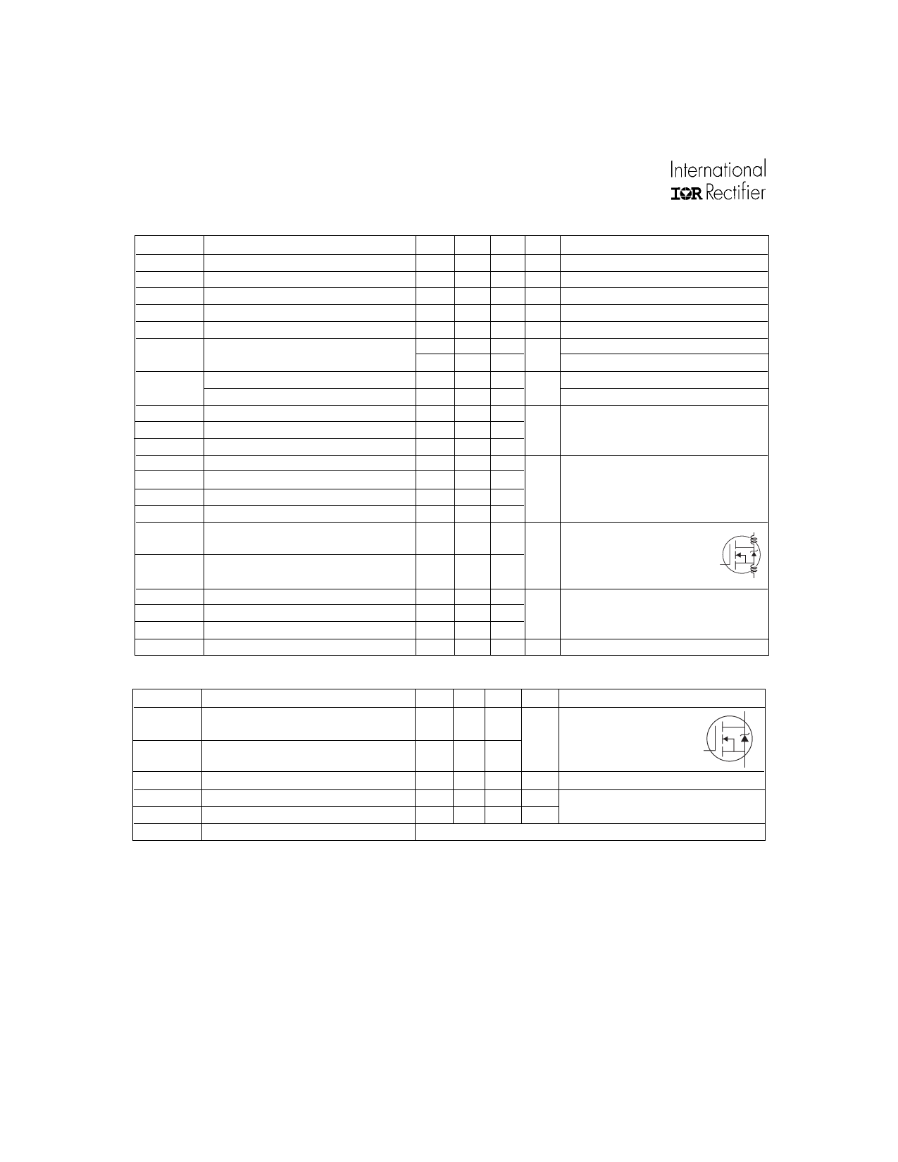
Electrical Characteristics @ TJ = 25°C (unless otherwise specified)
V(BR)DSS
∆V(BR)DSS/∆TJ
RDS(on)
VGS(th)
gfs
Parameter
Drain-to-Source Breakdown Voltage
Breakdown Voltage Temp. Coefficient
Static Drain-to-Source On-Resistance
Gate Threshold Voltage
Forward Transconductance
IDSS
Drain-to-Source Leakage Current
IGSS
Qg
Qgs
Qgd
td(on)
tr
td(off)
tf
Gate-to-Source Forward Leakage
Gate-to-Source Reverse Leakage
Total Gate Charge
Gate-to-Source Charge
Gate-to-Drain ("Miller") Charge
Turn-On Delay Time
Rise Time
Turn-Off Delay Time
Fall Time
LD
Internal Drain Inductance
LS
Internal Source Inductance
Ciss
Input Capacitance
Coss
Output Capacitance
Crss
Reverse Transfer Capacitance
EAS
Single Pulse Avalanche Energy
Min. Typ. Max. Units
Conditions
55 ––– ––– V VGS = 0V, ID = 250µA
––– 0.057 ––– V/°C Reference to 25°C, ID = 1mA
––– ––– 8.0 mΩ VGS = 10V, ID = 62A
2.0 ––– 4.0 V VDS = VGS, ID = 250µA
44 ––– ––– S VDS = 25V, ID = 62A
––– ––– 25
––– ––– 250
µA VDS = 55V, VGS = 0V
VDS = 44V, VGS = 0V, TJ = 150°C
––– ––– 100 nA VGS = 20V
––– ––– -100
VGS = -20V
––– ––– 146
ID = 62A
––– ––– 35 nC VDS = 44V
––– ––– 54
VGS = 10V, See Fig. 6 and 13
––– 14 –––
VDD = 28V
––– 101 ––– ns ID = 62A
––– 50 –––
RG = 4.5Ω
––– 65 –––
VGS = 10V, See Fig. 10
Between lead,
D
––– 4.5 –––
6mm (0.25in.)
nH
from package
G
––– 7.5 –––
and center of die contact
S
––– 3247 –––
VGS = 0V
––– 781 –––
VDS = 25V
––– 211 ––– pF ƒ = 1.0MHz, See Fig. 5
––– 1050 264 mJ IAS = 62A, L = 138µH
Source-Drain Ratings and Characteristics
Parameter
IS
Continuous Source Current
(Body Diode)
ISM
Pulsed Source Current
(Body Diode)
VSD
Diode Forward Voltage
trr
Reverse Recovery Time
Qrr
Reverse Recovery Charge
ton
Forward Turn-On Time
Notes:
Repetitive rating; pulse width limited by
max. junction temperature. ( See fig. 11 )
Starting TJ = 25°C, L = 138µH
RG = 25Ω, IAS = 62A. (See Figure 12)
ISD ≤ 62A, di/dt ≤ 207A/µs, VDD ≤ V(BR)DSS,
TJ ≤ 175°C
Min. Typ. Max. Units
Conditions
MOSFET symbol
D
––– ––– 110
A showing the
integral reverse
G
––– ––– 390
p-n junction diode.
S
––– ––– 1.3 V TJ = 25°C, IS = 62A, VGS = 0V
––– 69 104 ns TJ = 25°C, IF = 62A
––– 143 215 nC di/dt = 100A/µs
Intrinsic turn-on time is negligible (turn-on is dominated by LS+LD)
Pulse width ≤ 400µs; duty cycle ≤ 2%.
Calculated continuous current based on maximum allowable
junction temperature. Package limitation current is 75A.
This is a typical value at device destruction and represents
operation outside rated limits.
This is a calculated value limited to TJ = 175°C.
* When mounted on 1" square PCB ( FR-4 or G-10 Material ).
For recommended footprint and soldering techniques refer to application note #AN-994.
2
www.irf.com
Share Link: 