IRF3808S Ver la hoja de datos (PDF) - International Rectifier
Número de pieza
componentes Descripción
Lista de partido
IRF3808S Datasheet PDF : 11 Pages
| |||
IRF3808S/IRF3808L
Electrical Characteristics @ TJ = 25°C (unless otherwise specified)
Parameter
Min. Typ. Max. Units
Conditions
V(BR)DSS
∆V(BR)DSS/∆TJ
RDS(on)
VGS(th)
gfs
Drain-to-Source Breakdown Voltage
Breakdown Voltage Temp. Coefficient
Static Drain-to-Source On-Resistance
Gate Threshold Voltage
Forward Transconductance
IDSS
Drain-to-Source Leakage Current
IGSS
Qg
Qgs
Qgd
td(on)
tr
td(off)
tf
Gate-to-Source Forward Leakage
Gate-to-Source Reverse Leakage
Total Gate Charge
Gate-to-Source Charge
Gate-to-Drain ("Miller") Charge
Turn-On Delay Time
Rise Time
Turn-Off Delay Time
Fall Time
LD
Internal Drain Inductance
LS
Ciss
Coss
Crss
Coss
Coss
Coss eff.
Internal Source Inductance
Input Capacitance
Output Capacitance
Reverse Transfer Capacitance
Output Capacitance
Output Capacitance
Effective Output Capacitance U
75 ––– –––
––– 0.086 –––
––– 5.9 7.0
2.0 ––– 4.0
100 ––– –––
––– ––– 20
––– ––– 250
––– ––– 200
––– ––– -200
––– 150 220
––– 31 47
––– 50 76
––– 16 –––
––– 140 –––
––– 68 –––
––– 120 –––
––– 4.5 –––
––– 7.5 –––
––– 5310 –––
––– 890 –––
––– 130 –––
––– 6010 –––
––– 570 –––
––– 1140 –––
V
V/°C
mΩ
V
S
µA
nA
nC
ns
nH
pF
VGS = 0V, ID = 250µA
Reference to 25°C, ID = 1mA
VGS = 10V, ID = 82A T
VDS = 10V, ID = 250µA
VDS = 25V, ID = 82A
VDS = 75V, VGS = 0V
VDS = 60V, VGS = 0V, TJ = 150°C
VGS = 20V
VGS = -20V
ID = 82A
VDS = 60V
VGS = 10VT
VDD = 38V
ID = 82A
RG = 2.5Ω
VGS = 10V T
Between lead,
D
6mm (0.25in.)
from package
G
and center of die contact
S
VGS = 0V
VDS = 25V
ƒ = 1.0MHz, See Fig. 5
VGS = 0V, VDS = 1.0V, ƒ = 1.0MHz
VGS = 0V, VDS = 60V, ƒ = 1.0MHz
VGS = 0V, VDS = 0V to 60V
Source-Drain Ratings and Characteristics
Parameter
IS
Continuous Source Current
(Body Diode)
ISM
Pulsed Source Current
(Body Diode) Q
VSD
Diode Forward Voltage
trr
Reverse Recovery Time
Qrr
Reverse RecoveryCharge
ton
Forward Turn-On Time
Notes:
Q Repetitive rating; pulse width limited by
max. junction temperature. (See fig. 11).
R Starting TJ = 25°C, L = 0.130mH
RG = 25Ω, IAS = 82A. (See Figure 12).
S ISD ≤ 82A, di/dt ≤ 310A/µs, VDD ≤ V(BR)DSS,
TJ ≤ 175°C
T Pulse width ≤ 400µs; duty cycle ≤ 2%.
2
Min. Typ. Max. Units
Conditions
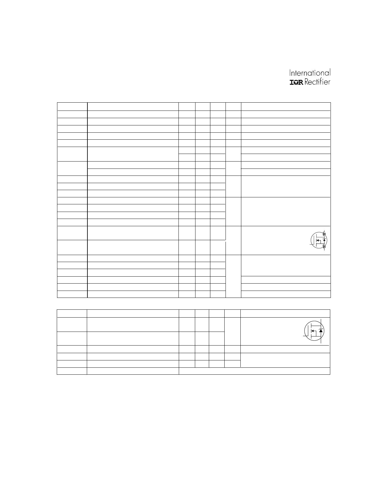
MOSFET symbol
D
––– ––– 106V
A
showing the
integral reverse
G
––– ––– 550
p-n junction diode.
S
––– ––– 1.3 V TJ = 25°C, IS = 82A, VGS = 0VT
––– 93 140 ns TJ = 25°C, IF = 82A
––– 340 510 nC di/dt = 100A/µsT
Intrinsic turn-on time is negligible (turn-on is dominated by LS+LD)
U Coss eff. is a fixed capacitance that gives the same charging time
as Coss while VDS is rising from 0 to 80% VDSS .
V Calculated continuous current based on maximum allowable
junction temperature. Package limitation current is 75A.
W Limited by TJmax , see Fig.12a, 12b, 15, 16 for typical repetitive
avalanche performance.
** When mounted on 1" square PCB ( FR-4 or G-10 Material ).
For recommended footprint and soldering techniques refer to
application note #AN-994.
www.irf.com
Share Link: 