GS88237BB-250V Ver la hoja de datos (PDF) - Giga Semiconductor
Número de pieza
componentes Descripción
Lista de partido
GS88237BB-250V Datasheet PDF : 28 Pages
| |||
GS88237BB/D-xxxV
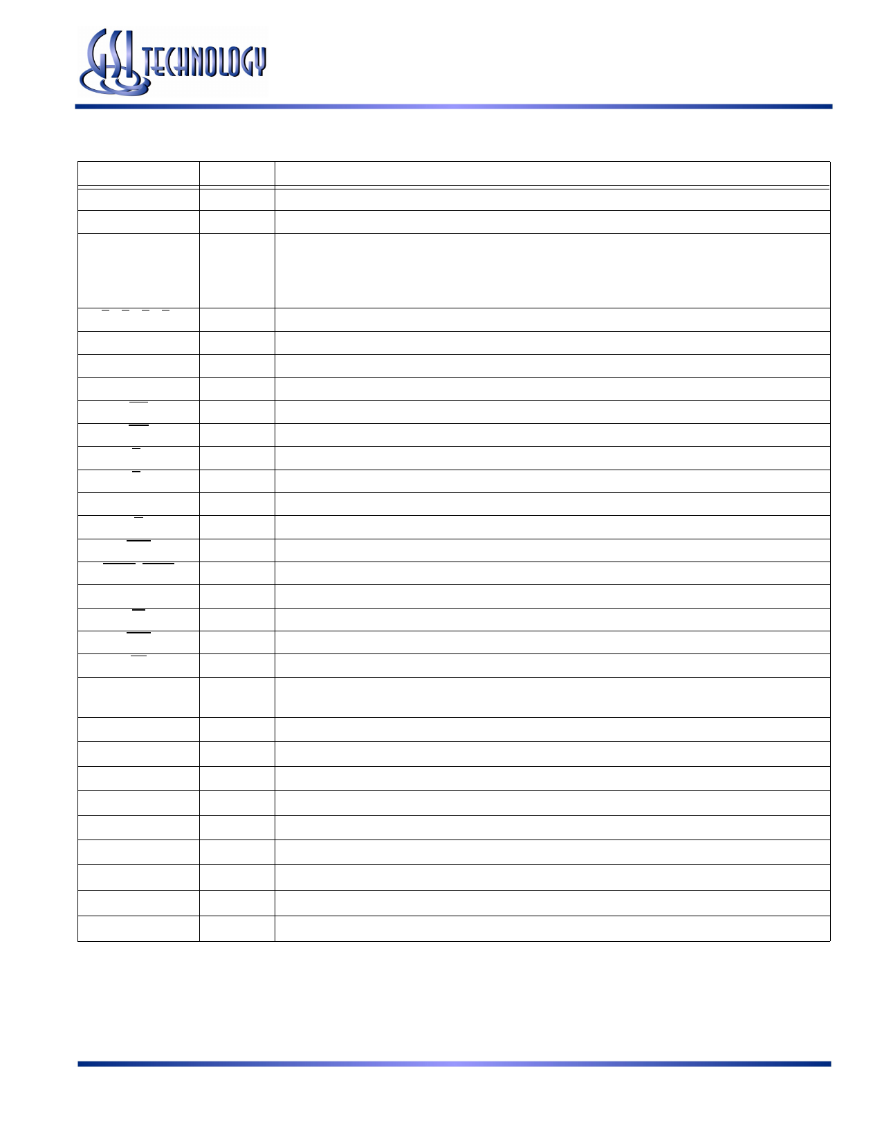
GS88237BB/D-xxxV BGA Pin Description
Symbol
A0, A1
A
DQA
DQB
DQC
DQD
BA, BB, BC, BD
NC
NC
CK
BW
GW
E1
E3
E2
G
ADV
ADSC, ADSP
ZZ
FT
LBO
PE
ZQ
TMS
TDI
TDO
TCK
MCL
SCD
VDD
VSS
VDDQ
Type
I
I
Description
Address field LSBs and Address Counter Preset Inputs
Address Inputs
I/O
Data Input and Output pins
I
Byte Write Enable for DQA, DQB, DQC, DQD I/Os; active low
—
No Connect
—
No Connect
I
Clock Input Signal; active high
I
Byte Write—Writes all enabled bytes; active low
I
Global Write Enable—Writes all bytes; active low
I
Chip Enable; active low
I
Chip Enable; active low
I
Chip Enable; active high
I
Output Enable; active low
I
Burst address counter advance enable; active l0w
I
Address Strobe (Processor, Cache Controller); active low
I
Sleep mode control; active high
I
Flow Through or Pipeline mode; active low
I
Linear Burst Order mode; active low
I
9th Bit Enable; active low (119-bump BGA only)
I
FLXDrive Output Impedance Control (Low = Low Impedance [High Drive], High = High Impedance [Low
Drive])
I
Scan Test Mode Select
I
Scan Test Data In
O
Scan Test Data Out
I
Scan Test Clock
—
Must Connect Low
—
Single Cycle Deselect/Dual Cyle Deselect Mode Control
I
Core power supply
I
I/O and Core Ground
I
Output driver power supply
Rev: 1.04 6/2006
4/28
Specifications cited are subject to change without notice. For latest documentation see http://www.gsitechnology.com.
© 2003, GSI Technology
Share Link: 