GS881Z18BD-150IV Ver la hoja de datos (PDF) - Giga Semiconductor
Número de pieza
componentes Descripción
Lista de partido
GS881Z18BD-150IV Datasheet PDF : 37 Pages
| |||
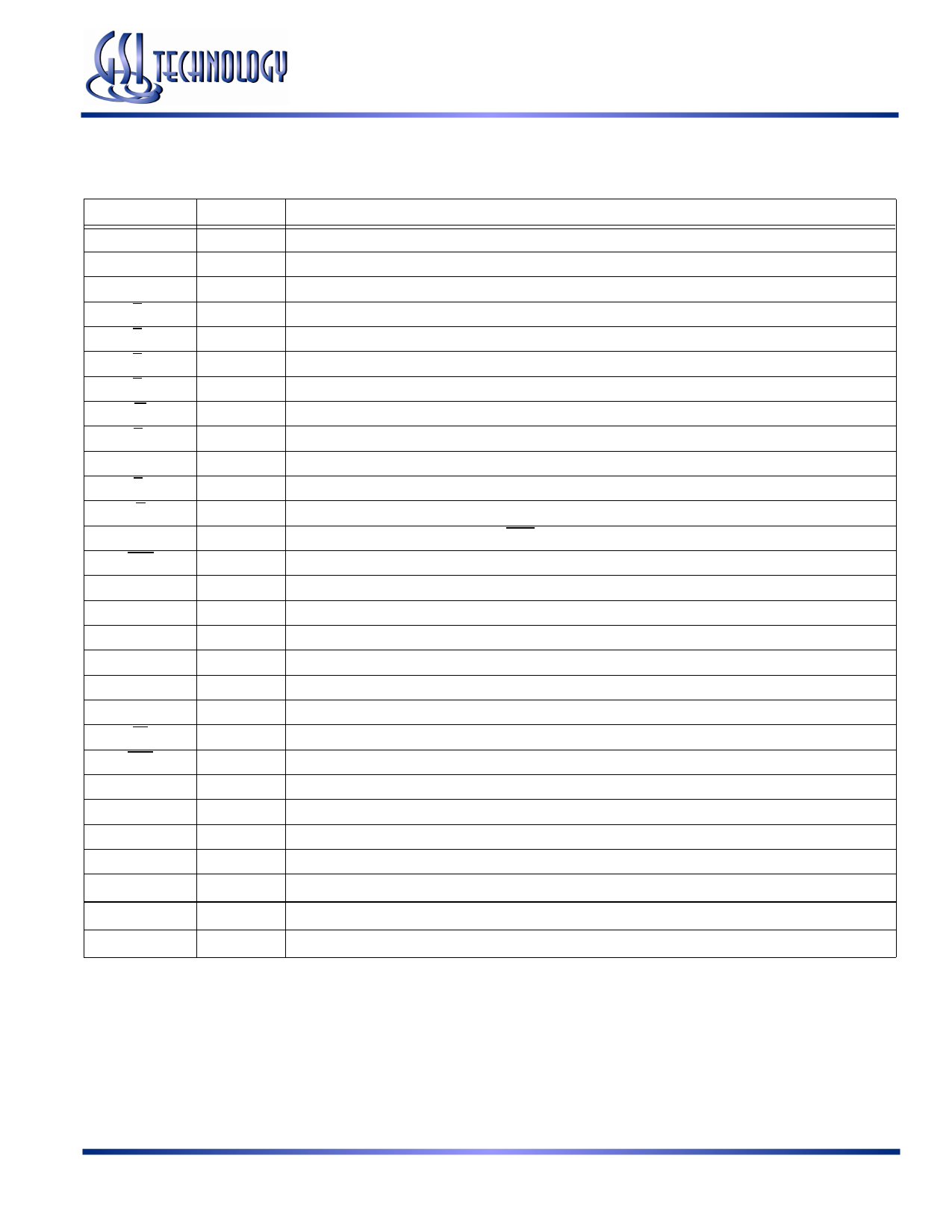
100-Pin TQFP Pin Descriptions
Symbol
A0, A1
A
CK
BA
BB
BC
BD
W
E1
E2
E3
G
ADV
CKE
NC
DQA
DQB
DQC
DQD
ZZ
FT
LBO
TMS
TDI
TDO
TCK
VDD
VSS
VDDQ
Type
In
In
In
In
In
In
In
In
In
In
In
In
In
In
—
I/O
I/O
I/O
I/O
In
In
In
In
In
In
GS881Z18/32/36B(T/D)-xxxV
Description
Burst Address Inputs; Preload the burst counter
Address Inputs
Clock Input Signal
Byte Write signal for data inputs DQA1–DQA9; active low
Byte Write signal for data inputs DQB1–DQB9; active low
Byte Write signal for data inputs DQC1–DQC9; active low
Byte Write signal for data inputs DQD1–DQD9; active low
Write Enable; active low
Chip Enable; active low
Chip Enable—Active High. For self decoded depth expansion
Chip Enable—Active Low. For self decoded depth expansion
Output Enable; active low
Advance/Load; Burst address counter control pin
Clock Input Buffer Enable; active low
No Connect
Byte A Data Input and Output pins
Byte B Data Input and Output pins
Byte C Data Input and Output pins
Byte D Data Input and Output pins
Power down control; active high
Pipeline/Flow Through Mode Control; active low
Linear Burst Order; active low.
Scan Test Mode Select
Scan Test Data In
Scan Test Data Out
Scan Test Clock
Core power supply
Ground
Output driver power supply
Rev: 1.00 6/2006
5/37
Specifications cited are subject to change without notice. For latest documentation see http://www.gsitechnology.com.
© 2006, GSI Technology
Share Link: 