ST75C530 Ver la hoja de datos (PDF) - STMicroelectronics
Número de pieza
componentes Descripción
Lista de partido
ST75C530
SUPER INTEGRATED DEVICES WITH DSP, AFE & MEMORIES FORTELEPHONY, MODEM, FAX OVERINTERNET & POTS LINES
STMicroelectronics

ST75C530 Datasheet PDF : 84 Pages
| |||
ST75C530 - ST75C540
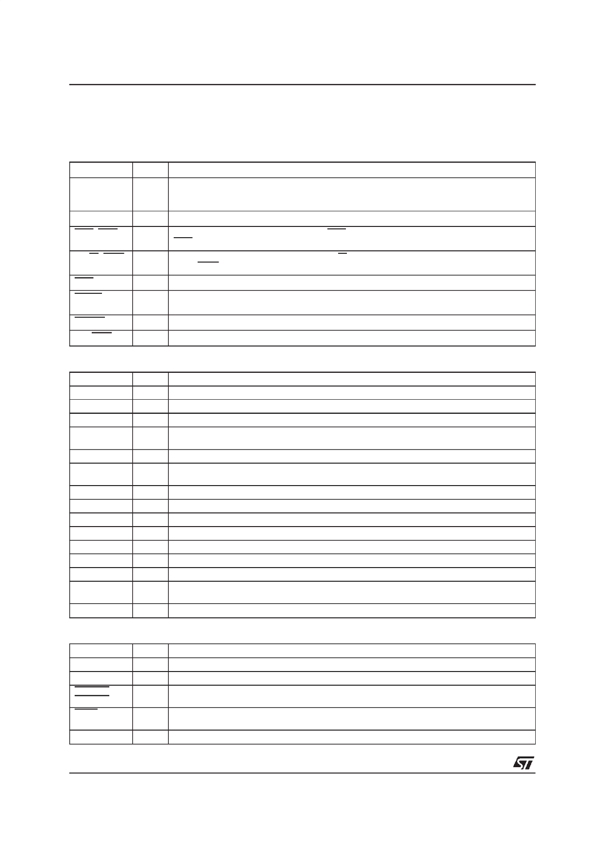
II - PIN DESCRIPTION (continued)
II.2 - Host Interface
The exchanges with the control processor proceed through a 128 x 8 DUAL port RAM shared between the
ST75C530/540 and the Host. The signals associated with this interface are :
Pin Name Type
Description
SD0..SD7
I/O System Data Bus. 8-bit data bus used for asynchronous exchanges between the
ST75C530/540 and the Host through the dual port RAM. High impedance when exchanges
are not active.
SA0..SA6
I System Address Bus. 7-bit address bus for dual port RAM, IO and interrupt registers.
SDS (SRD)
I System Data Strobe. In Motorola mode SDS initiates the exchange, active low. In Intel mode
SRD initiates a read exchange, active low.
SR/W (SWR)
I
System Read/Write. In Motorola mode SR/W defines the type of exchange read/write. In Intel
mode SWR initiates a write exchange, active low.
SCS
I System Chip Select. Active low.
SINTR
OD System Interrupt Request. Open drain. Active low. This signal isasserted by the ST75C530/540
and negated by the host.
RESET
I Reset. Active low.
INT/MOT
I Select Intel or Motorola Interface
II.3 - Analog Interface
Pin Name
TxA1
TxA2
RxA
SPK1P
SPK1N
SPK2P
SPK2N
SPK3P
SPK3N
MIC1
MIC2
MIC3
VCM
VREFN
VREFP
Type
O
O
I
O
O
O
O
O
O
I
I
I
I/O
I
I
Description
Transmit Analog Output 1
Transmit Analog Output 2
Receive Analog Input
Speaker Output 1, (differential positive), must be connected through Amplifier to the
loudspeaker.
Speaker Output 1, (differential negative)
Speaker Output 2, (differential positive), must be connected through Amplifier to the Handset
loudspeaker.
Speaker Output 2, (differential negative)
Speaker Output 3, (differential positive)
Speaker Output 3, (differential negative)
Microphone Input 1
Microphone Input 2
Microphone Input 3
Analog Common Voltage (nominal +2.5V). This input must be decoupled with respect to AGND.
Analog Negative Reference (nominal 1.25V). This input must be decoupled with respect to
VCM.
Analog Positive Reference (nominal 3.75V). This input must be decoupled with respect to VCM.
II.4 - General Purpose IO and Relay
Pin Name
GIO[0,7]
GIO[10,17]
RELAY0,
RELAY1
RING
RGND
Type
I/O
I/O
OD
Description
General Purpose I/O Pins, can be independently selected as input or output.
General Purpose I/O Pins, can be independently selected as input or output.
Relay Outputs, Open Drain, Active Low. Can sink -10mA to RGND.
I
PWR
Ring detect signal. Active low. If the ST75C530/540 is in low power mode, a low level will awake
the chip. This input is a Schmidt’s trigger.
Relay Digital Ground. To connect to GND.
6/84
Share Link: