L4937NL Ver la hoja de datos (PDF) - STMicroelectronics
Número de pieza
componentes Descripción
Lista de partido
L4937NL Datasheet PDF : 9 Pages
| |||
L4937N
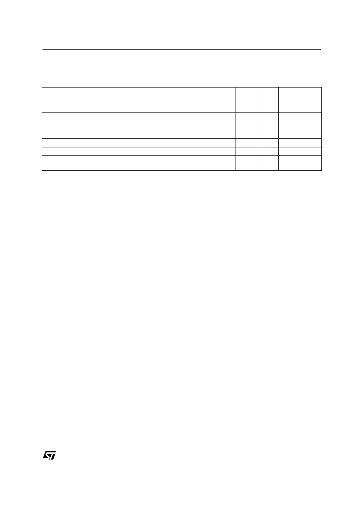
ELECTRICAL CHARACTERISTICS (continued)
RESET
Symbol
Parameter
Test Conditions
Min. Typ. Max. Unit
VRt
VRth
tRD
tRR
VRL
ILRES
VCTth
VCTth, hyst
Reset Low Threshold Voltage
Reset Threshold Hysteresis
Reset Pulse Delay
Reset Reaction Time
Reset Output LOW Voltage
Reset Output HIGH Leakage
Delay Comparator Threshold
Delay Comparator Threshold
Hysteresis
VS = 14V
CT = 100nF; tR > 100µs
CT = 100nF
RRES = 10KΩ to V01 VS ≥ 1.5V
VRES = 5V
Vo1 -0.4 4.7 Vo1 -0.1 V
50
100 200 mV
55
100 180
ms
1
10
50
µs
0.4
V
1
µA
2.0
V
100
mV
Note : 1 : VO2 connected to ADJ.VO2 can be set to higher values by inserting an external resistor divider.
2 : Foldback characteristic
t(s) FUNCTIONAL DESCRIPTION
The L4937N is based on the SGS-THOMSON Mi-
c croelectronics modular voltage regulator approach.
u Several out-standing features and auxiliary func-
rod tions are provided to meet the requirements of sup-
plying the microprocessor systems used in automo-
P tive applications.
te Furthermore the device is suitable also in other ap-
le plications requiring two stabilized voltages.
o The modular approach allows other features and
s functions to be realized easily when required.
Ob STANDBY REGULATOR
- The standby regulator uses an Isolated Collector
t(s) Vertical PNP transistor as the regulating element.
This structure allows a very low dropout voltage at
c currents up to 50mA. The dropout operation of the
u standby regulator is maintained down to 2V input
d supply voltage. The output voltage is regulated up
ro to the transient input supply voltage of 40V. This fea-
P ture avoids functional interruptions which could be
Obsolete generated by overvoltage pulses.
The typical curve of the standby output voltage as
a function of the input supply voltage is shown in fig.
1.
The current consumption of the device (quiescent
current) is less than 250µA when output 2 is dis-
abled (standby mode). The dropout voltage is con-
trolled to reduce the quiescent current peak in the
undervoltage region and to improve the transient
response in this region.
The quiescent current is shown in fig. 2 as a function
of the supply input voltage 2.
OUTPUT 2 VOLTAGE
The output 2 regulator uses the same output struc-
ture as the standby regulator, but rated for an output
current of 500mA.
The output 2 regulator works in tracking mode with
the standby output voltage as a reference voltage.
The output 2 regulator can be switched off via the
Enable input.
5/9
Share Link: 