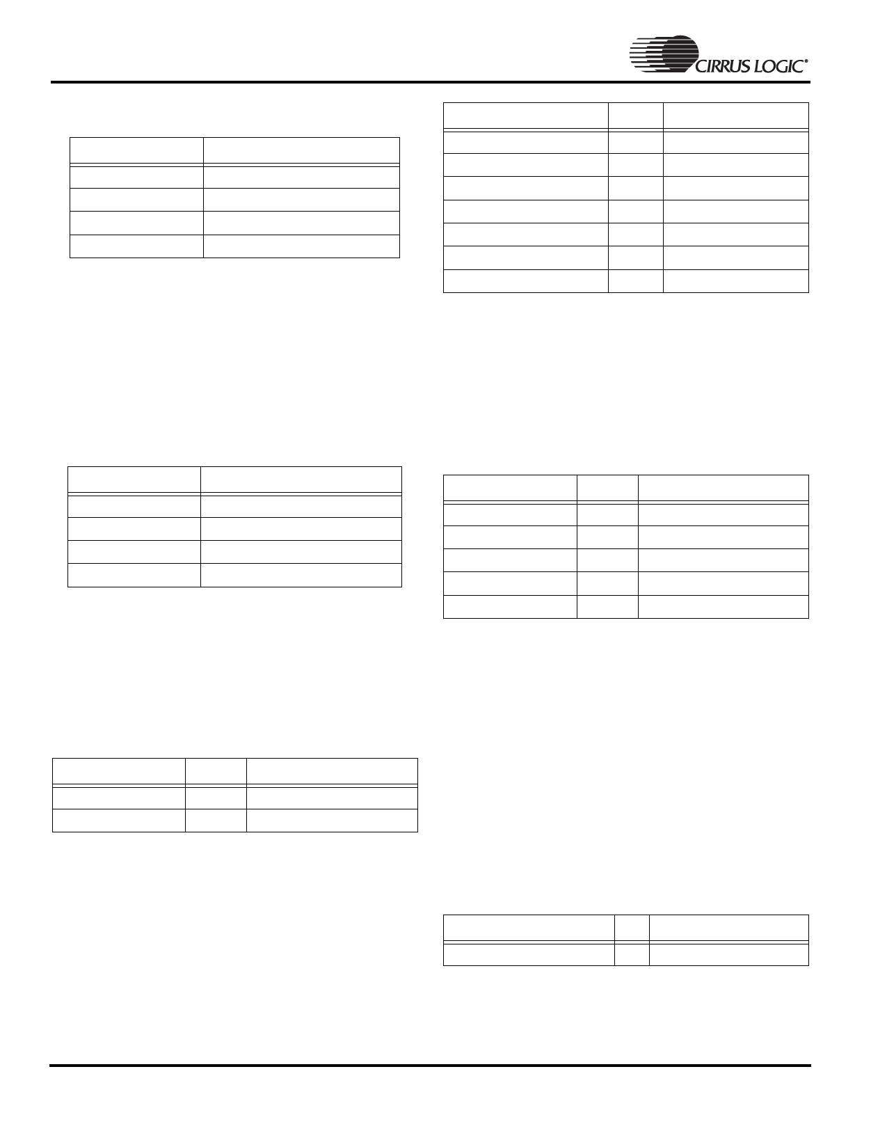
EP7309-EB-C Ver la hoja de datos (PDF) - Cirrus Logic
Número de pieza
componentes Descripción
Lista de partido
EP7309-EB-C Datasheet PDF : 46 Pages
| |||
EP7309
High-Performance, Low-Power System on Chip
• Driven byan external 32.768 kHz crystal oscillator
Pin Mnemonic
Pin Description
RTCIN
RTCOUT
VDDRTC
VSSRTC
Real-Time Clock Oscillator Input
Real-Time Clock Oscillator Output
Real-Time Clock Oscillator Power
Real-Time Clock Oscillator Ground
Table K. Real-Time Clock Pin Assignments
PLL and Clocking
• Processor and Peripheral Clocks operate from a single
3.6864 MHz crystal or external 13 MHz clock
• Programmable clock speeds allow the peripheral bus
to run at 18 MHz when the processor is set to 18 MHz
and at 36 MHz when the processor is set to 36, 49 or
74 MHz
Pin Mnemonic
I/O
Pin Description
PA[7:0]
I
GPIO port A
PB[7:0]
I
GPIO port B
PD[0]/LEDFLSH
(Note) I/O GPIO port D
PD[5:1]
I/O GPIO port D
PD[7:6]/SDQM[1:0] (Note) I/O GPIO port D
PE[1:0]/BOOTSEL[1:0] (Note)
I
GPIO port E
PE[2]/CLKSEL
(Note)
I
GPIO port E
Table N. General Purpose Input/Output Pin Assignments
Note: Pins are multiplexed. See Table R on page 7 for more
information.
Hardware debug Interface
• Full JTAG boundary scan and Embedded ICE
support
Pin Mnemonic
Pin Description
MOSCIN
MOSCOUT
VDDOSC
VSSOSC
Main Oscillator Input
Main Oscillator Output
Main Oscillator Power
Main Oscillator Ground
Table L. PLL and Clocking Pin Assignments
DC-to-DC converter interface (PWM)
• Provides two 96 kHz clock outputs with
programmable duty ratio (from 1-in-16 to 15-in-16)
that can be used to drive a positive or negative DC to
DC converter
Pin Mnemonic
I/O
Pin Description
DRIVE[1:0]
FB[1:0]
I/O PWM drive output
I
PWM feedback input
Table M. DC-to-DC Converter Interface Pin Assignments
Timers
• Internal (RTC) timer
• Two internal 16-bit programmable hardware count-
down timers
General Purpose Input/Output (GPIO)
• Three 8-bit and one 3-bit GPIO ports
• Supports scanning keyboard matrix
Pin Mnemonic
I/O
Pin Description
TCLK
TDI
TDO
nTRST
TMS
I
JTAG clock
I
JTAG data input
O
JTAG data output
I
JTAG async reset input
I
JTAG mode select
Table O. Hardware Debug Interface Pin Assignments
LED Flasher
A dedicated LED flasher module can be used to generate
a low frequency signal on Port D pin 0 for the purpose of
blinking an LED without CPU intervention. The LED
flasher feature is ideal as a visual annunciator in battery
powered applications, such as a voice mail indicator on a
portable phone or an appointment reminder on a PDA.
• Software adjustable flash period and duty cycle
• Operates from 32 kHz RTC clock
• Will continue to flash in IDLE and STANDBY states
• 4 mA drive current
Pin Mnemonic
I/O
Pin Description
PD[0]/LEDFLSH
(Note) O LED flasher driver
Table P. LED Flasher Pin Assignments
Note: Pins are multiplexed. See Table R on page 7 for more
information.
6
Copyright 2001 Cirrus Logic (All Rights Reserved)
DS507PP1
Share Link: 