CXA1744AR Ver la hoja de datos (PDF) - Sony Semiconductor
Número de pieza
componentes Descripción
Lista de partido
CXA1744AR Datasheet PDF : 18 Pages
| |||
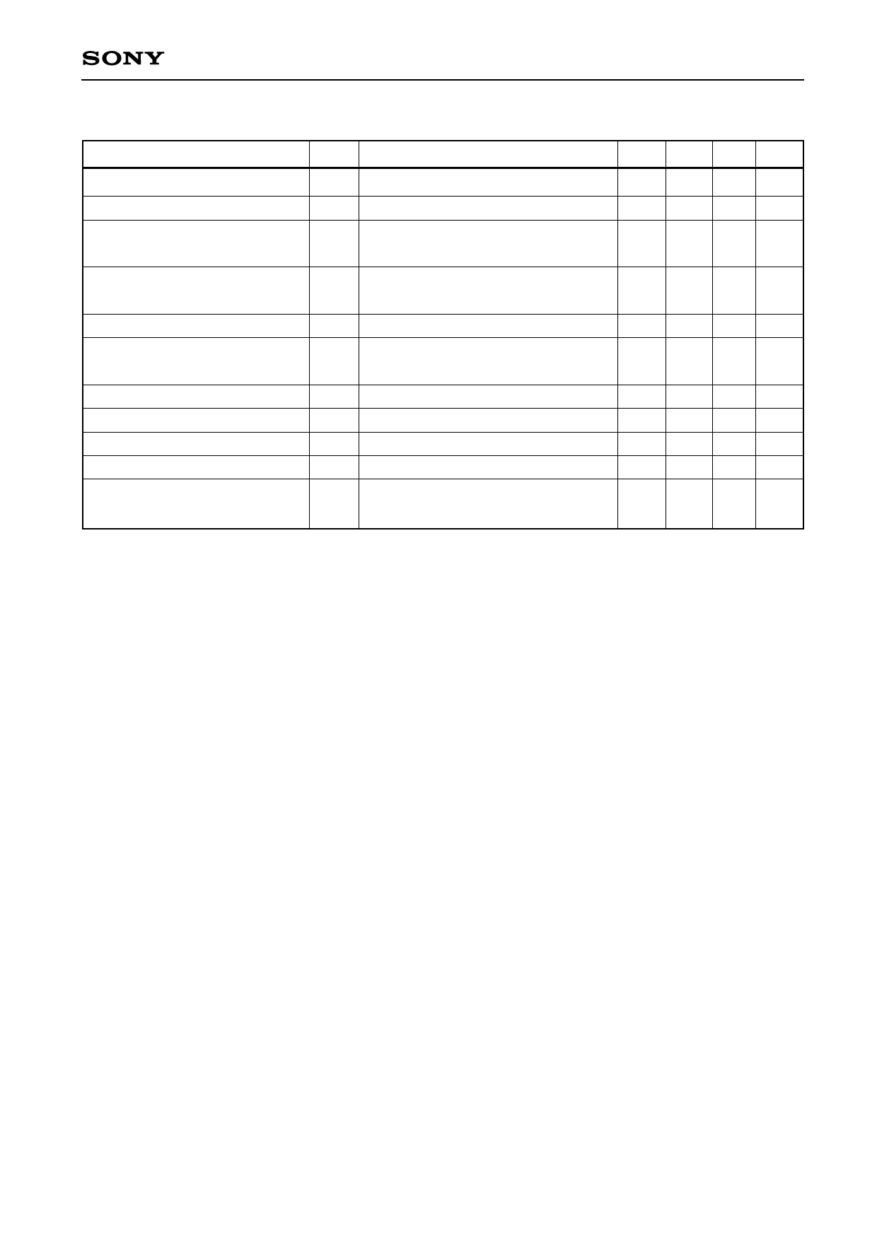
CXA1744AR
Design Reference Values
Item
Symbol
Conditions
Multiplier output amplitude
3rd order intercepting point
RF input impedance
S11 real component
RF input impedance
S11 imaginary component
Mixer noise figure
IF amplifier voltage
gain difference (for adjustment)
RSSI rise time
RSSI fall time
RSSI rise time
RSSI fall time
Input sensitivity
(12 dB SINAD value)
VMLT fin=27.87MHz, -10dBm
IP3
fin=150.05MHz
fin=150.05MHz
SBB conversion
RL=470Ω, difference to Pin 29 open
For input signal OFF/ON
For input signal ON/OFF
For burst operation
For burst operation
For MIXIN input (50Ω LC matching)
(50Ω LC matching)
(VCC=3.0V, Ta=25°C)
Min. Typ. Max. Unit
— 200 — mVP-P
— -8 — dBM
— 145 — Ω
— -380 — Ω
— 11 — dB
— 3 — dB
— 30 — µsec
— 50 — µsec
— 40 — µsec
— 40 — µsec
— 4.5 — µV
—10—
Share Link: 