MC74VHC540DTR2G(2011) Ver la hoja de datos (PDF) - ON Semiconductor
Número de pieza
componentes Descripción
Lista de partido
MC74VHC540DTR2G Datasheet PDF : 7 Pages
| |||
MC74VHC540
Octal Bus Buffer
Inverting
The MC74VHC540 is an advanced high speed CMOS inverting
octal bus buffer fabricated with silicon gate CMOS technology. It
achieves high speed operation similar to equivalent Bipolar Schottky
TTL while maintaining CMOS low power dissipation.
The MC74VHC540 features inputs and outputs on opposite sides
of the package and two AND−ed active−low output enables. When
either OE1 or OE2 are high, the terminal outputs are in the high
impedance state.
The internal circuit is composed of three stages, including a buffer
output which provides high noise immunity and stable output. The
inputs tolerate voltages up to 7.0 V, allowing the interface of 5.0 V
systems to 3.0 V systems.
Features
• High Speed: tPD = 3.7 ns (Typ) at VCC = 5.0 V
• Low Power Dissipation: ICC = 4.0 μA (Max) at TA = 25°C
• High Noise Immunity: VNIH = VNIL = 28% VCC
• Power Down Protection Provided on Inputs
• Balanced Propagation Delays
• Designed for 2.0 V to 5.5 V Operating Range
• Low Noise: VOLP = 1.2 V (Max)
• Pin and Function Compatible with Other Standard Logic Families
• Latchup Performance Exceeds 300 mA
• ESD Performance: HBM > 2000 V; Machine Model > 200 V
• Chip Complexity: 124 FETs or 31 Equivalent Gates
• These Devices are Pb−Free and are RoHS Compliant
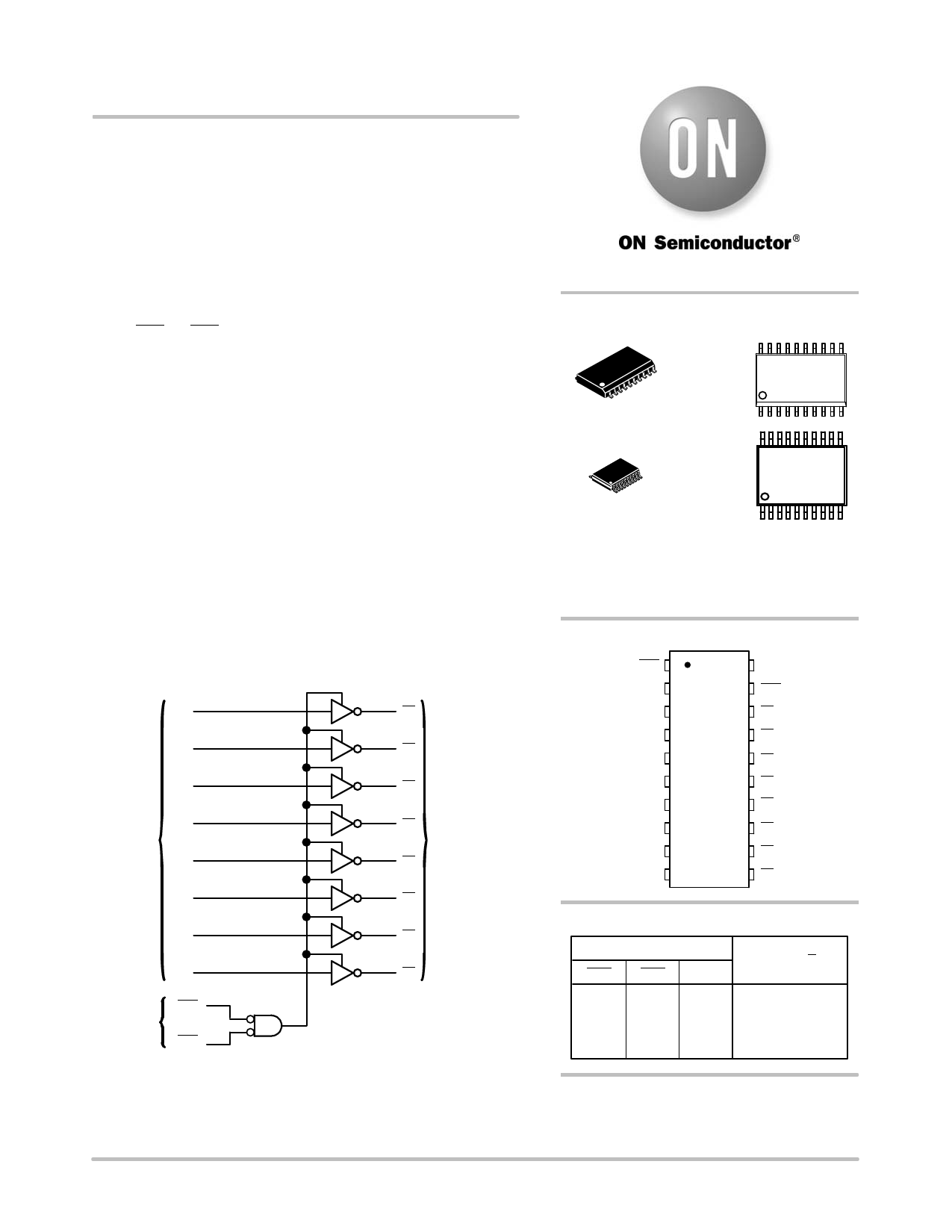
DATA
INPUTS
OUTPUT
ENABLES
2
A1
18
Y1
3
A2
17
Y2
4
A3
16
Y3
5
A4
6
A5
15
Y4
14
Y5
INVERTING
OUTPUTS
7
A6
13
Y6
8
A7
12
Y7
9
A8
OE1 1
11
Y8
OE2 19
Figure 1. Logic Diagram
© Semiconductor Components Industries, LLC, 2011
1
May, 2011 − Rev. 5
http://onsemi.com
MARKING
DIAGRAMS
20
1
1
SOIC−20
DW SUFFIX
CASE 751D
VHC540
AWLYYWWG
20
1
TSSOP−20
DT SUFFIX
CASE 948E
VHC
540
ALYWG
G
A
= Assembly Location
WL, L = Wafer Lot
YY, Y = Year
WW, W = Work Week
G or G = Pb−Free Package
PIN ASSIGNMENT
OE1 1
A1 2
A2 3
A3 4
A4 5
A5 6
A6 7
A7 8
A8 9
GND 10
20 VCC
19 OE2
18 Y1
17 Y2
16 Y3
15 Y4
14 Y5
13 Y6
12 Y7
11 Y8
FUNCTION TABLE
Inputs
OE1 OE2
A
Output Y
L
L
L
H
L
L
H
L
H
X
X
Z
X
H
X
Z
ORDERING INFORMATION
See detailed ordering and shipping information in the package
dimensions section on page 5 of this data sheet.
Publication Order Number:
MC74VHC540/D
Share Link: 