IMIC9835 Ver la hoja de datos (PDF) - Cypress Semiconductor
Número de pieza
componentes Descripción
Lista de partido
IMIC9835
Cypress Semiconductor

IMIC9835 Datasheet PDF : 18 Pages
| |||
C9835
Maximum Ratings
Maximum Input Voltage Relative to VSS: ............ VSS – 0.3V
Maximum Input Voltage Relative to VDD:............. VDD + 0.3V
Storage Temperature: ................................–65°C to + 150°C
Operating Temperature: .................................... 0°C to +85°C
Maximum ESD Protection.............................................. 2 KV
Maximum Power Supply: ................................................5.5V
This device contains circuitry that protects the inputs against
damage due to high static voltages or electric field; however,
precautions should be taken to avoid application of any
voltage higher than the maximum rated voltages to this circuit.
For proper operation, VIN and VOUT should be constrained to
the range:
VSS < (VIN or VOUT) < VDD.
Unused inputs must always be tied to an appropriate logic
voltage level (either VSS or VDD).
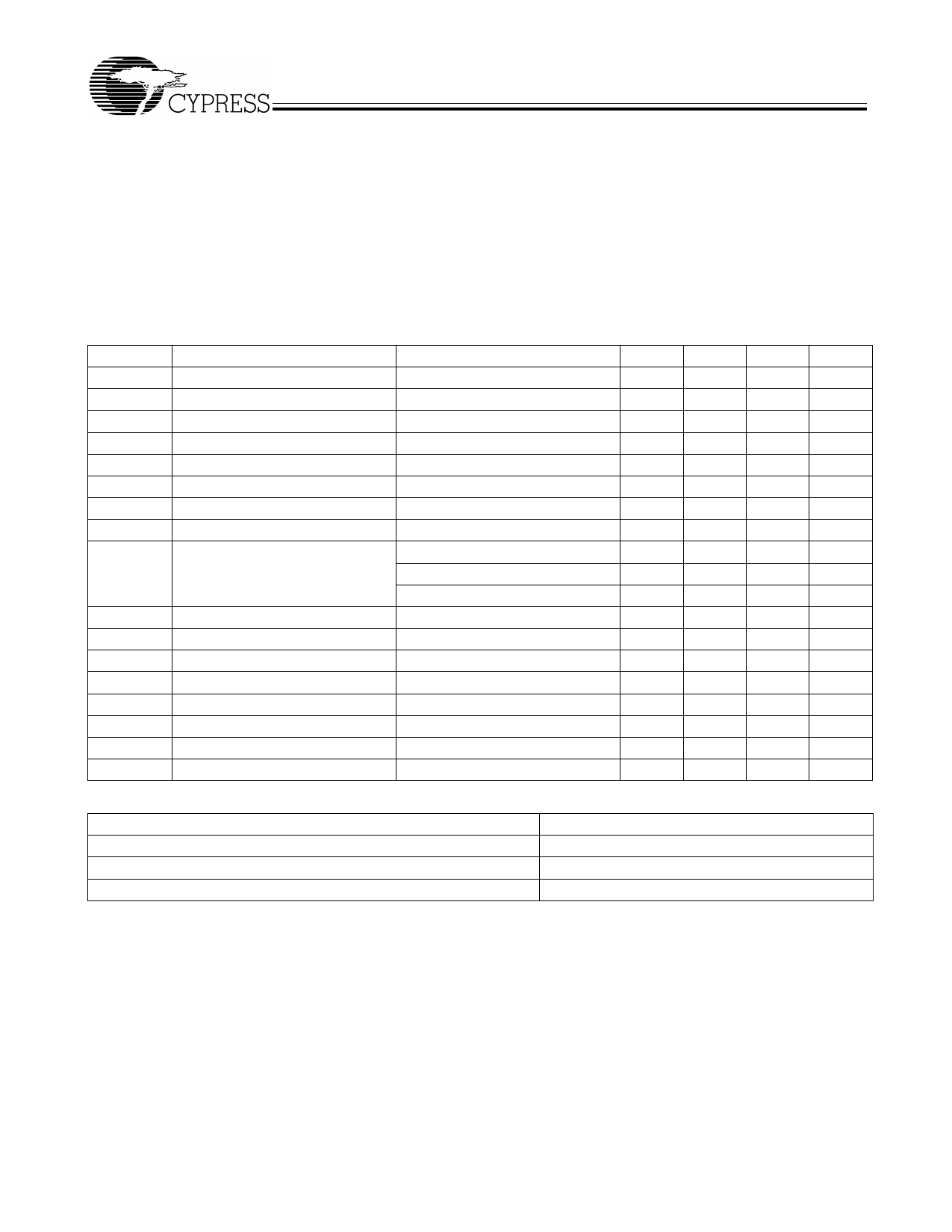
DC Parameters VDD = VDDS = 3.3V ± 5%, VDDC = VDDI = 2.5V ± 5%, TA = 0°C to +70°C[20]
Parameter
Description
Conditions
Min. Typ. Max. Units
VIL1
Input Low Voltage
Note 21
1.0
V
VIH1
Input High Voltage
2.0
V
VIL2
Input Low Voltage
Note 22
1.0
V
VIH2
IIL1
IIH1
Ioz
Input High Voltage
2.2
Input Low Current (@VIL = VSS)
For internal pull-up resistors[23]
Input High Current (@VIH =VDD)
Three-state leakage Current
V
–20
µA
20
µA
10
µA
Idd3.3V
Dynamic Supply Current
295
mA
Idd2.5V
CPU @ 66 MHz
60
mA
Dynamic Supply Current
CPU @ 100 MHz
75
mA
CPU @ 133 MHz
90
mA
Ipd3.3V
Power Down Supply Current
PD# = “0”
1
mA
Ipd2.5V
Power Down Supply Current
PD# = “0”
1
mA
Cin
Input pin capacitance
5
pF
Cout
Output pin capacitance
6
pF
Lpin
Cxtal
Pin inductance
Crystal pin capacitance
7
nH
Measured from Pin to Ground[24]
34
36
38
pF
VBIAS
Txs
Crystal DC Bias Voltage
Crystal Startup time
0.3VDD VDD/2 0.7VDD
V
From stable 3.3V power supply.
40
µs
Table 7. Maximum Output Load
Clock Name
CPU(0:2), IOAPIC(0:1), REF, 48M0 (USB), VCH_CLK
PCI(0:6), SDRAM(0:5), DCLK, 3V66(0:2)
48M1 (DOT)
Max Load (in pF)
20
30
15
Notes:
20. All outputs loaded per Table 7.
21. Applicable to input signals : SEL(0:1), PD# (pull-up).
22. Applicable to SDATA and SCLK.
23. Internal pull-up and pull-down resistors affect this current.
24. See Applications data that is presented later in this datasheet on crystal interfacing.
Document #: 38-07303 Rev. **
Page 11 of 18
Share Link: