HV9606DB1 Ver la hoja de datos (PDF) - Supertex Inc
Número de pieza
componentes Descripción
Lista de partido
HV9606DB1 Datasheet PDF : 4 Pages
| |||
Instructions
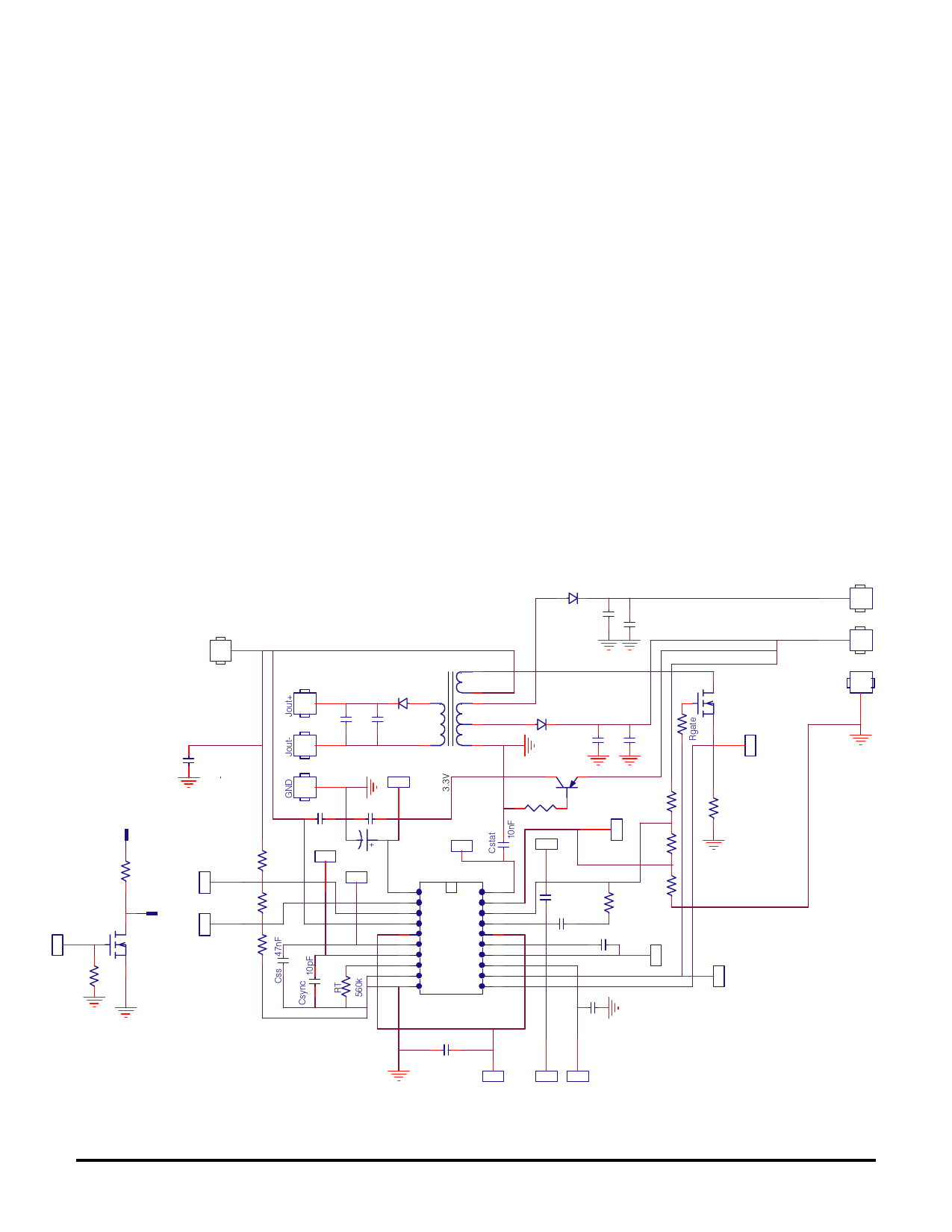
Vin , GND
Connect 21 to 100V power source to these terminals:
positive to Vin , negative to GND.
3.3VREG, GND
Connect your load to these terminals. This is a
regulated 3.3V output. This output can typically
deliver a current up to 106mA.
5.0VREG, GND
Connect your load to these terminals. This is a 5.0V
output. This output can typically deliver a current up
to 30mA.
Schematic Diagram
HV9606DB1
JOUT+, JOUT-
Connect your load to these terminals. This is an
isolated 40.0V output. This output can typically
deliver a current up to 12.5mA.
ON/OFF
This is a remote inhibit pin. Connecting this pin to
GND will disable the converter. The converter will
resume operation beginning with soft start as the
ON/OFF pin is released.
PWRGD
This is an active "High", remote power-good
indicator. This pin is utilized with CMOS coupled logic
of 3.3V for "High" and 0V for "Low".
EXT SYNC
Apply external clock, a 3.3 volt logic signal to Ext
Sync. Clock frequency has to exceed 25kHz to sync,
but not exceed 50kHz.
Vin
Cin2
33uF, 450V
VDD
R12
1K
Ext Sync
M3
10k
R16
STOP
To S ync Pin
START
2N7000
R5+ R4
12.2M
R6+ R2
2.0M
R7+ R3
5.7M
D1
+
SK15
1nF
C3
C4
4700uF
VOUT3 (Isolated)
C5
1nF
D4
DL4002
3
+
Cout
100uF
1
TX1 9
W4 8
12
W3 11
W1
W2 10
VDD
3.3nF 1nF C9
C10
Sync
C1
4.7uF
SS
1
2
3
4
5
6
7
8
9
10
STATUS
20
19
18
17
16
15
14
13
12
11
HV9606
CREF
1uF
D2
SK15
+
C2
4700uF
Q1
M1
TN2524
10
1nF
C8
CS
R17
26.1K SENSE
FB
C7
330pF
3.3nF
R9
62.4K
R10
2.61K
R11
35K
R1
100k
C6 10nF CCA
CB
Rsense
1
GATE
100nF
CVX2
Ref
COMP VX2
5.0V
3.3VRE
GND
2
09/05/2002
Supertex, Inc. 1235 Bordeaux Drive, Sunnyvale, CA 94089 TEL: (408) 744-0100 FAX: (408) 222-4895 www.supertex.com
Share Link: 