HD74HC353 Ver la hoja de datos (PDF) - Renesas Electronics
Número de pieza
componentes Descripción
Lista de partido
HD74HC353 Datasheet PDF : 7 Pages
| |||
HD74HC353
Dual 4-to-1-line Data Selectors/Multiplexers
REJ03D0612–0200
(Previous ADE-205-491)
Rev.2.00
Jan 31, 2006
Description
Each of these data selectors/multiplexers contains inverters and drivers to supply full binary decoding data selection to
the AND-OR-invert gates. Separate strobe inputs (G) are provided for each of the two four-line sections.
The three-state outputs can interface with and drive data lines of bus-organized systems. With all but one of the
common output disabled (at a high-impedance state) the low-impedance of the single enable output will drive the bus
line to a high or low logic level. Each output has its own strobe (G). The output is disabled when its strobe is high.
Features
• High Speed Operation: tpd (Data to Y) = 13 ns typ (CL = 50 pF)
• High Output Current: Fanout of 10 LSTTL Loads
• Wide Operating Voltage: VCC = 2 to 6 V
• Low Input Current: 1 µA max
• Low Quiescent Supply Current: ICC (static) = 4 µA max (Ta = 25°C)
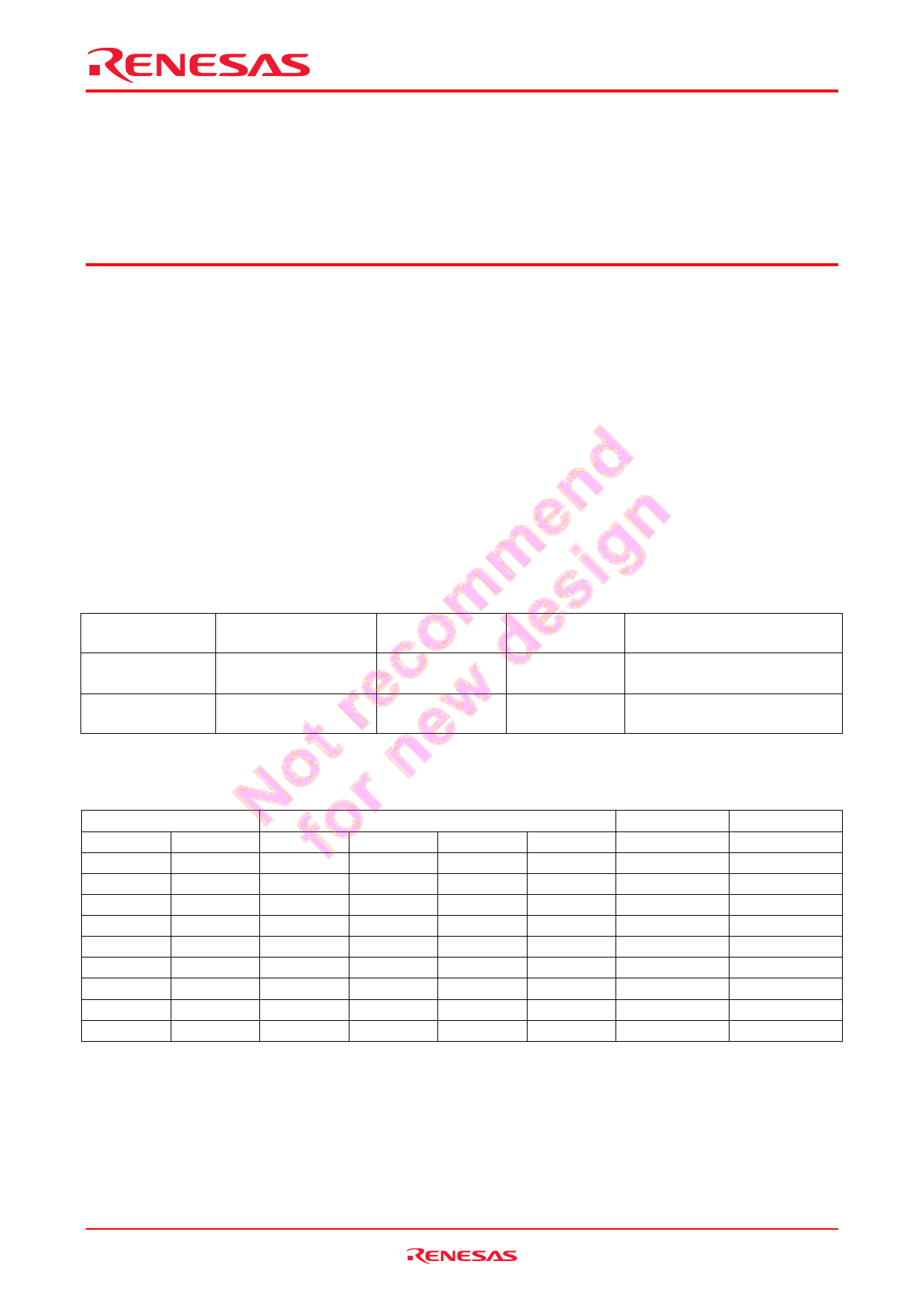
• Ordering Information
Part Name
Package Type
Package Code
(Previous Code)
Package
Abbreviation
HD74HC353P
DILP-16 pin
PRDP0016AE-B
P
(DP16FV)
HD74HC353RPEL SOP-16 pin (JEDEC)
PRSP0016DG-A
(FP-16DNV)
RP
Note: Please consult the sales office for the above package availability.
Taping Abbreviation
(Quantity)
—
EL (2,500 pcs/reel)
Function Table
Select Input
Data Inputs
B
A
C0
C1
C2
X
X
X
X
X
L
L
L
X
X
L
L
H
X
X
L
H
X
L
X
L
H
X
H
X
H
L
X
X
L
H
L
X
X
H
H
H
X
X
X
H
H
X
X
X
Select inputs A and B are common to both sections
Output Control
Output
C3
G
Y
X
H
Z
X
L
H
X
L
L
X
L
H
X
L
L
X
L
H
X
L
L
L
L
H
H
L
L
Rev.2.00 Jan 31, 2006 page 1 of 6
Share Link: 