MB86615PFV Ver la hoja de datos (PDF) - Fujitsu
Número de pieza
componentes Descripción
Lista de partido
MB86615PFV Datasheet PDF : 48 Pages
| |||
MB86615
s PIN DESCRIPTION
1. 1394 Interface
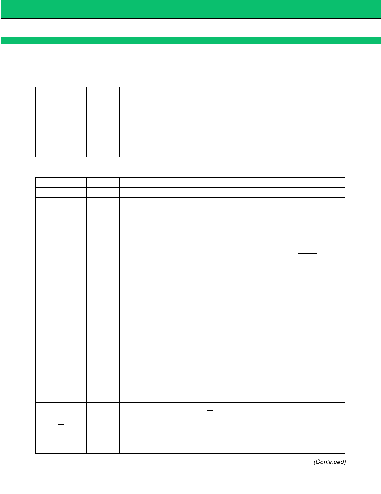
Pin name
TPA
TPA
TPB
TPB
TPBIAS
ROI
I/O
Function
I/O 1394 Cable port TPA positive signal I/O pin
I/O 1394 Cable port TPA negative signal I/O pin
I/O 1394 Cable port TPB positive signal I/O pin
I/O 1394 Cable port TPB negative signal I/O pin
O 1394 Cable port common voltage reference voltage output pin
O
Connect to GND through 4.7 kΩ resistance
2. Isochronous-data Interface
Pin name
ICLK
IDIR
ILWRE
ID7 to ID0
IV
I/O
Function
I
Isochronous data interface CLK signal input pin (4 MHz to 16 MHz).
Isochronous transfer transmission/reception switching signal input pin.
0 input: The device clears the ISO-FIFO buffer and enters the transmission
mode.
The device asserts the ILWRE signal and starts transmission after
receiving one packet of data according to the “data-length” setting
(bank 0: 10h).
I
1 input: The device clears the ISO-FIFO buffer and enters the reception mode.
If any packet being transmitted exists, the device enters the reception
mode after completing transmission of the packet. The ILWRE signal is
asserted upon reception of one packet.
Note: The IDIR signal should normally be left at “1” and switched to “0” only for
transmission.
ISO-FIFO access enable signal output pin.
Transmission mode: The signal is asserted when the FIFO buffer is not full.
The signal is negated when the FIFO buffer becomes full.
When it is negated, data is accepted only up to the rising
edge of the next ICLK signal.
When a bus reset is detected, the signal is negated after
accepting data of up to the packet boundary.
O
After the bus reset, the signal is asserted again upon
completion of transmission of one source packet remaining
in the FIFO buffer.
Reception mode: The signal is asserted upon completion of one packet of data.
The signal is negated once when one packet of data is read
from the FIFO buffer and asserted back if the FIFO buffer still
contains any packet of data which has been received
completely.
I/O Isochronous transfer data input/output bits. (MSB is ID7, LSB is ID0)
ID7 to ID0 enable signal input pin
Transmission mode: While the IV signal is active, data from the ID7 to ID0 pins is
loaded into the ISO-FIFO buffer at the rising edge of the
I
ICLK signal.
Reception mode: While the signal becomes active, the device starts sending
data from the ISO-FIFO buffer to the ID7 to ID0 pins. Data is
then switched at the rising edge of the ICLK signal.
(Continued)
9
Share Link: 