CD74HC373 Ver la hoja de datos (PDF) - Philips Electronics
Número de pieza
componentes Descripción
Lista de partido
CD74HC373 Datasheet PDF : 8 Pages
| |||
Philips Semiconductors
24-bit bus switch with 12-bit output enables
Product data
CBT16211
AC CHARACTERISTICS
GND = 0 V; tR; CL = 50 pF
SYMBOL
PARAMETER
FROM
(INPUT)
TO
(OUTPUT)
VCC = 5.0 V ±0.5 V
Min
Max
UNIT
tpd
Propagation delay1
A or B
B or A
—
0.25
ns
ten
Output enable time
to High and Low level
OE
A or B
1.5
6.0
ns
tdis
Output disable time
from High and Low level
OE
A or B
1.5
6.0
ns
NOTE:
1. This parameter is warranted but not production tested. The propagation delay is based on the RC time constant of the typical on-state
resistance of the switch and a load capacitance of 50 pF, when driven by an ideal voltage source (zero output impedance).
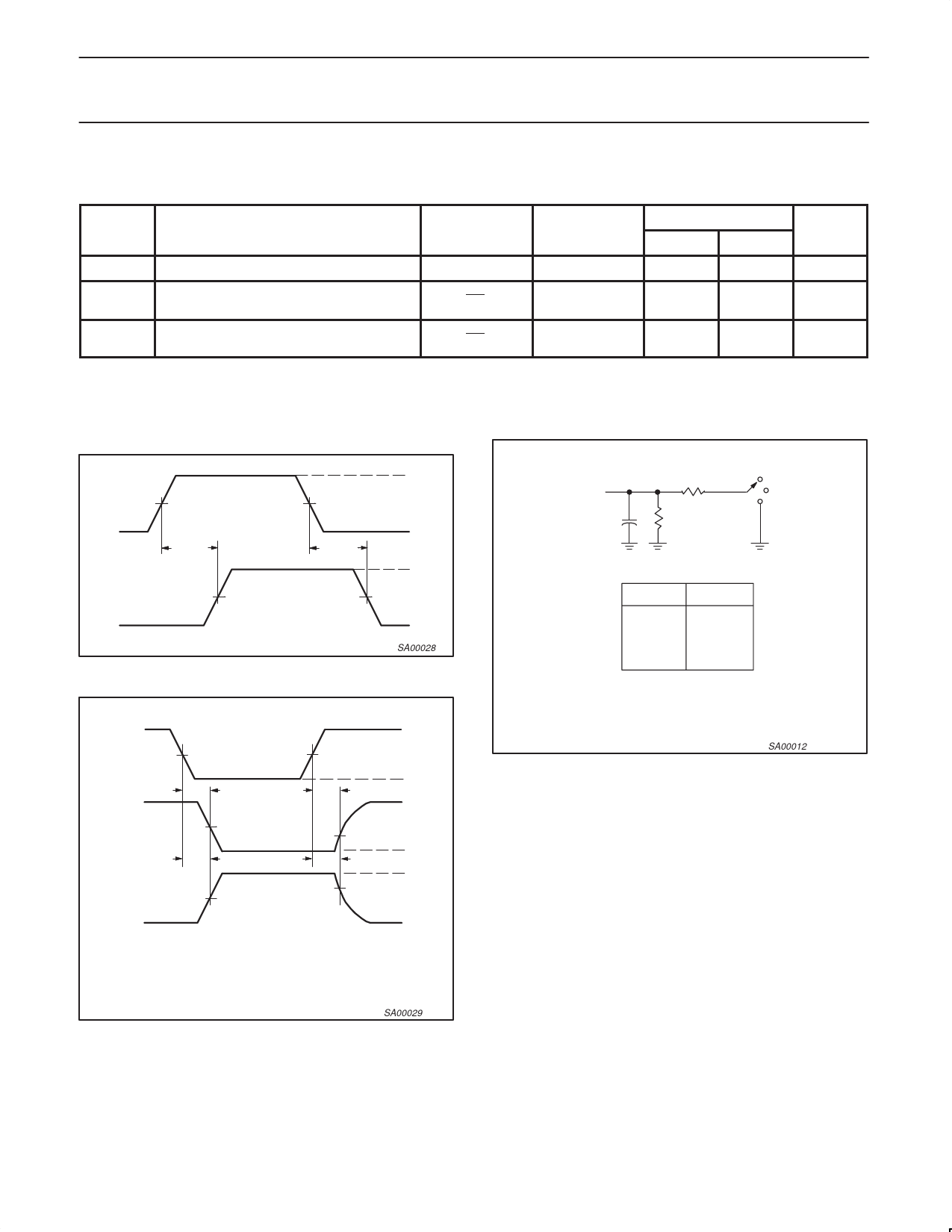
AC WAVEFORMS
VM = 1.5 V, VIN = GND to 3.0 V.
3V
INPUT
1.5 V
tPLH
1.5 V
tPHL
0V
VOH
OUTPUT
1.5 V
1.5 V
VOL
SA00028
Waveform 1. Input (An) to Output (Yn) Propagation Delays
Output Control
(Low-level
enabling )
1.5 V
3V
1.5 V
tPZL
Output
Waveform 1
S1 at 7 V
(see Note)
tPZH
Output
Waveform 2
S1 at Open
(see Note)
1.5 V
1.5 V
tPLZ
tPHZ
0V
3.5 V
VOL + 0.3 V
VOL
VOH
VOH – 0.3 V
0V
Note:
Waveform 1 is for an output with internal conditions such that
the output is low except when disabled by the output control.
Waveform 2 is for an output with internal conditions such that
the output is high except when disabled by the output control.
SA00029
Waveform 2. 3-State Output Enable and Disable Times
TEST CIRCUIT AND WAVEFORMS
From Output
Under Test
CL = 50 pF
500 Ω
500 Ω
7V
S1
Open
GND
Load Circuit
TEST
S1
tpd
tPLZ/tPZL
tPHZ/tPZH
open
7V
open
DEFINITIONS
CL = Load capacitance includes jig and probe capacitance;
see AC CHARACTERISTICS for value.
SA00012
2001 Jun 13
5
Share Link: 