MPC2605ZP66R Ver la hoja de datos (PDF) - Motorola => Freescale
Número de pieza
componentes Descripción
Lista de partido
MPC2605ZP66R Datasheet PDF : 30 Pages
| |||
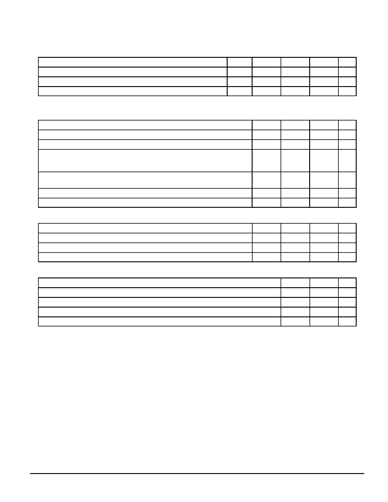
DC OPERATING CONDITIONS AND CHARACTERISTICS
(TJ = 20 to + 110°C, Unless Otherwise Noted)
RECOMMENDED OPERATING CONDITIONS (Voltages Referenced to VSS = 0 V)
Parameter
Symbol
Min
Typ
Supply Voltage (Operating Voltage Range)
VDD
3.135
3.3
Input High Voltage
Input Low Voltage
* VIL(min) = – 2.0 V ac (pulse width ≤ 20 ns).
VIH
2.0
—
VIL
– 0.5*
—
DC CHARACTERISTICS
Parameter
Symbol
Min
Input Leakage Current (All Inputs, Vin = 0 to VDD)
Ilkg(I)
—
Output Leakage Current (High–Z State, Vout = 0 to VDD)
Ilkg(O)
—
AC Supply Current (Iout = 0 mA, All inputs = VIL or VIH, VIL = 0 V, and VIH ≥ 3.0 V,
ICCA
—
Cycle Time = 15 ns, max value assumes a constant burst read hit, with 100% bus utilization,
and 100% hit rate)
AC Quiescent Current (Iout = 0 mA, All inputs = VIL or VIH, VIL = 0 V and VIH ≥ 3.0 V,
Cycle Time = 15 ns, All Other Inputs DC)
IQ
—
Output Low Voltage (IOL = + 8.0 mA)
Output High Voltage (IOH = – 4.0 mA)
VOL
—
VOH
2.4
CAPACITANCE (f = 1.0 MHz, dV = 3.0 V, TA = 25°C, Periodically Sampled Rather Than 100% Tested)
Parameter
Symbol
Typ
Input Capacitance
Output Capacitance
Cin
4
Cout
6
Input/Output Capacitance
CI/O
8
PACKAGE THERMAL CHARACTERISTICS
Rating
Thermal Resistance Junction to Ambient (Still Air, Test Board with Two Internal Planes)
Thermal Resistance Junction to Ambient (200 lfpm, Test Board with Two Internal Planes)
Thermal Resistance Junction to Board (Bottom)
Thermal Resistance Junction to Case (Top)
Symbol
RθJA
RθJA
RθJB
RθJC
Max
Unit
3.465
V
5.5
V
0.8
V
Max
Unit
± 1.0
µA
± 1.0
µA
720
mA
195
mA
0.4
V
—
V
Max
Unit
6
pF
8
pF
10
pF
Max
Unit
26.5 °C/W
23.2 °C/W
15.9 °C/W
6.6
°C/W
MPC2605
6
MOTOROLA
Share Link: 