HM-6518-9 Ver la hoja de datos (PDF) - Intersil
Número de pieza
componentes Descripción
Lista de partido
HM-6518-9 Datasheet PDF : 7 Pages
| |||
HM-6518
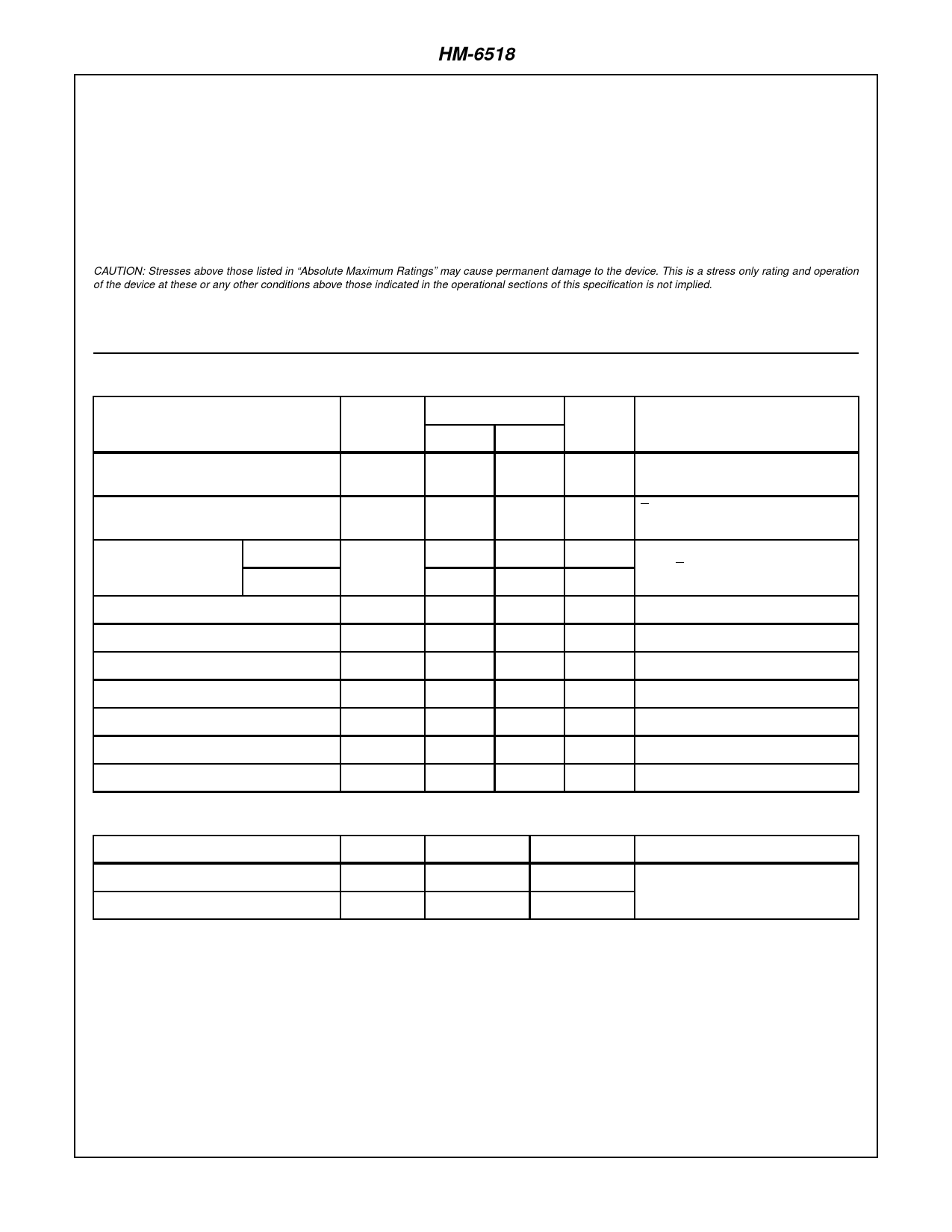
Absolute Maximum Ratings
Supply Voltage . . . . . . . . . . . . . . . . . . . . . . . . . . . . . . . . . . . . . +7.0V
Input, Output or I/O Voltage . . . . . . . . . . . GND -0.3V to VCC +0.3V
ESD Classification . . . . . . . . . . . . . . . . . . . . . . . . . . . . . . . . Class 1
Operating Conditions
Operating Voltage Range . . . . . . . . . . . . . . . . . . . . . +4.5V to +5.5V
Operating Temperature Range
HM-6518B-9, HM-6518-9 . . . . . . . . . . . . . . . . . . . -40oC to +85oC
Thermal Information
Thermal Resistance (Typical, Note 1)
θJA
θJC
CERDIP Package . . . . . . . . . . . . . . . . 75oC/W
15oC/W
Maximum Storage Temperature Range . . . . . . . . .-65oC to +150oC
Maximum Junction Temperature . . . . . . . . . . . . . . . . . . . . . . +175oC
Maximum Lead Temperature (Soldering 10s) . . . . . . . . . . . . +300oC
Die Characteristics
Gate Count . . . . . . . . . . . . . . . . . . . . . . . . . . . . . . . . . . . 1936 Gates
CAUTION: Stresses above those listed in “Absolute Maximum Ratings” may cause permanent damage to the device. This is a stress only rating and operation
of the device at these or any other conditions above those indicated in the operational sections of this specification is not implied.
NOTE:
1. θJA is measured with the component mounted on an evaluation PC board in free air.
DC Electrical Specifications VCC = 5V ±10%; TA = -40oC to +85oC (HM-6518B-9, HM-6518-9)
LIMITS
PARAMETER
SYMBOL
MIN
MAX
UNITS
TEST CONDITIONS
Standby Supply Current
ICCSB
-
Operating Supply
Current (Note 1)
ICCOP
-
Data Retention Supply HM-6518B-9
ICCDR
-
Current
HM-6518-9
-
10
µA
IO = 0mA, VI = VCC or GND,
VCC = 5.5V
4
mA
E = 1MHz, IO = 0mA, VI = VCC or
GND, VCC = 5.5V
5
µA
VCC = 2.0V, IO = 0mA, VI = VCC or
GND, E = VCC
10
µA
Data Retention Supply Voltage
VCCDR
2.0
-
V
Input Leakage Current
Output Leakage Current
Input Low Voltage
Input High Voltage
Output Low Voltage
Output High Voltage
II
IOZ
VIL
VIH
VOL
VOH
-1.0
+1.0
-1.0
+1.0
-0.3
0.8
VCC -2.0
-
VCC +0.3
0.4
2.4
-
µA
VI = VCC or GND, VCC = 5.5V
µA
VO = VCC or GND, VCC = 5.5V
V
VCC = 4.5V
V
VCC = 5.5V
V
IO = 3.2mA, VCC = 4.5V
V
IO = -0.4mA, VCC = 4.5V
Capacitance TA = +25oC
PARAMETER
SYMBOL
Input Capacitance (Note 2)
CI
Output Capacitance (Note 2)
CO
NOTES:
1. Typical derating 1.5mA/MHz increase in ICCOP.
2. Tested at initial design and after major design changes.
MAX
6
10
UNITS
pF
pF
TEST CONDITIONS
f = 1MHz, All measurements are
referenced to device GND
6-3
Share Link: 