74AHC86BQ Ver la hoja de datos (PDF) - NXP Semiconductors.
Número de pieza
componentes Descripción
Lista de partido
74AHC86BQ Datasheet PDF : 14 Pages
| |||
Nexperia
74AHC86; 74AHCT86
Quad 2-input EXCLUSIVE-OR gate
Table 7. Dynamic characteristics …continued
GND = 0 V; For test circuit see Figure 7.
Symbol Parameter Conditions
25 °C
−40 °C to +85 °C −40 °C to +125 °C Unit
Min Typ[1] Max Min
Max
Min
Max
For type 74AHCT86
tpd
propagation nA, nB to nY; see Figure 6 [2]
delay
VCC = 4.5 V to 5.5 V
CL = 15 pF
- 3.4 6.9 1.0
8.0
1.0
9.0 ns
CL = 50 pF
- 4.9 8.8 1.0
10.0
1.0
11.0 ns
CPD
power
CL = 50 pF; fi = 1 MHz;
[3] - 12.0 -
-
-
-
-
pF
dissipation VI = GND to VCC
capacitance
[1] Typical values are measured at nominal supply voltage (VCC = 3.3 V and VCC = 5.0 V).
[2] tpd is the same as tPLH and tPHL.
[3] CPD is used to determine the dynamic power dissipation (PD in µW).
PD = CPD × VCC2 × fi × N + Σ(CL × VCC2 × fo) where:
fi = input frequency in MHz, fo = output frequency in MHz
CL = output load capacitance in pF
VCC = supply voltage in Volts
N = number of inputs switching
Σ(CL × VCC2 × fo) = sum of the outputs.
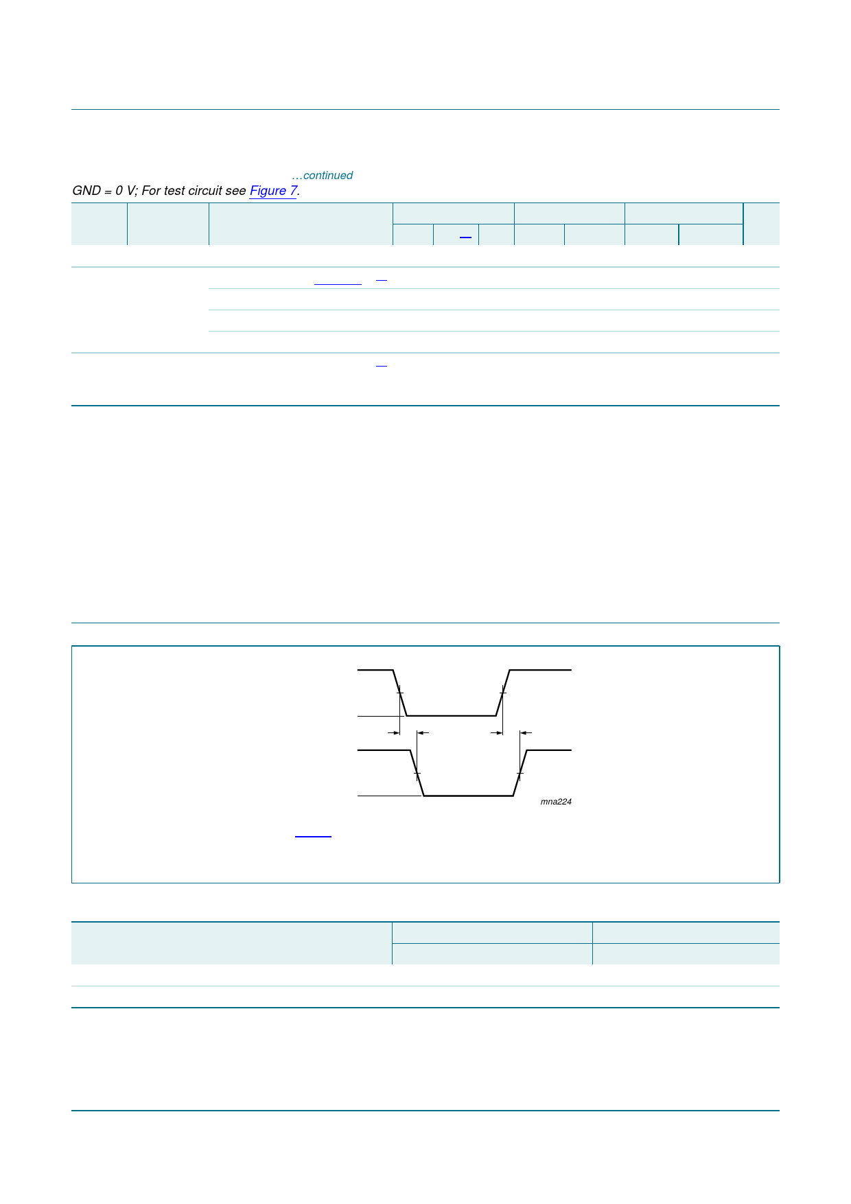
11. Waveforms
VI
nA, nB input
GND
VOH
nY output
VOL
VM
t PHL
VM
Measurement points are given in Table 8.
VOL and VOH are typical voltage output levels that occur with the output load.
Fig 6. Propagation delay input (nA, nB) to output (nY)
t PLH
mna224
Table 8. Measurement points
Type
74AHC86
74AHCT86
Input
VM
0.5VCC
1.5 V
Output
VM
0.5VCC
0.5VCC
74AHC_AHCT86_2
Product data sheet
Rev. 02 — 15 November 2007
© Nexperia B.V. 2017. All rights reserved
7 of 14
Share Link: 