ADAS3022BCPZ Ver la hoja de datos (PDF) - Analog Devices
Número de pieza
componentes Descripción
Lista de partido
ADAS3022BCPZ Datasheet PDF : 42 Pages
| |||
ADAS3022
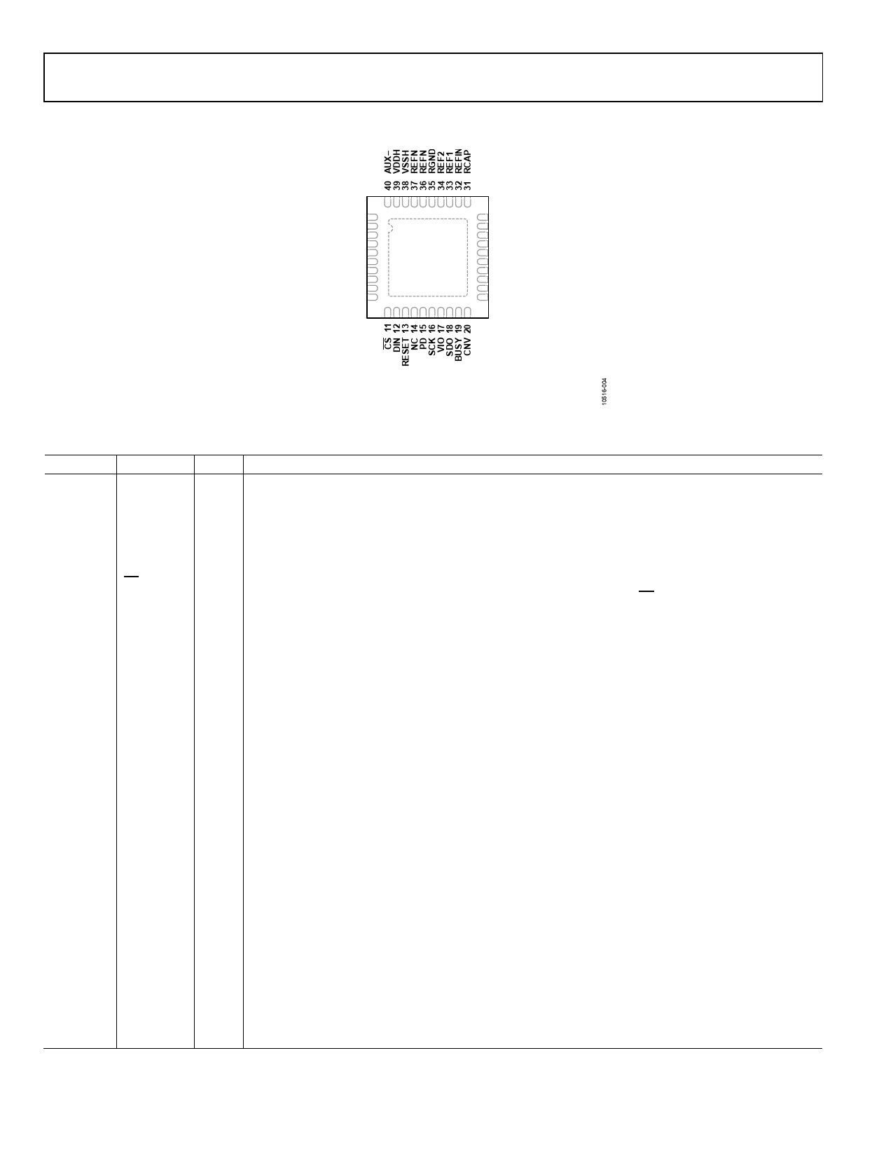
PIN CONFIGURATION AND FUNCTION DESCRIPTIONS
Data Sheet
IN0 1
IN1 2
IN2 3
IN3 4
AUX+ 5
IN4 6
IN5 7
IN6 8
IN7 9
COM 10
ADAS3022
TOP VIEW
(Not to Scale)
30 NC
29 NC
28 AVDD
27 DVDD
26 ACAP
25 DCAP
24 AGND
23 AGND
22 DGND
21 DGND
NOTES
1. NC = NO CONNECT. THIS PIN IS NOT INTERNALLY CONNECTED.
2. EXPOSED PADDLE. THE EXPOSED PADDLE MUST BE CONNECTED TO VSSH.
Figure 5. LFCSP Pin Configuration
Table 5. LFCSP Pin Function Descriptions
Pin No. Mnemonic Type1 Description
1 to 4
IN0 to IN3 AI
Input Channel 0 to Input Channel 3.
5
AUX+
AI
Auxiliary Input Channel Positive Input.
6 to 9
IN4 to IN7 AI
Input Channel 4 to Input Channel 7.
10
COM
AI
IN[7:0] Common Channel Input. The IN[7:0] input channels can be referenced to a common point. The
maximum voltage on this pin is ±10.24 V for all PGIA gains except for a PGIA gain of 0.16, in which case
the maximum voltage on this pin is ±12.228 V. AUX+ and AUX− are not referenced to COM.
11
CS
DI
Chip Select. Active low signal. Enables the digital interface for writing and reading data. Use this pin
when sharing the serial bus. For a dedicated ADAS3022 serial interface, CS can be tied to DGND or CNV
to simplify the interface.
12
DIN
DI
Data Input. Serial data input used for writing the 16-bit configuration word (CFG) that is latched on SCK
rising edges. CFG is an internal register that is updated on the rising edge of the end of a conversion, which is
the falling edge of BUSY. The configuration register can be written to during and after a conversion.
13
RESET
DI
Asynchronous Reset. A low-to-high transition resets the ADAS3022. The current conversion, if active, is
aborted and CFG is reset to the default state.
14, 29, 30 NC
NC No Connect. This pin is not connected internally.
15
PD
DI
Power-Down. A low-to-high transition powers down the ADAS3022, minimizing the bias current. Note
that this pin must be held high until the user is ready to power on the device; after powering on the
device, the user must wait 100 ms until the reference is enabled and then wait for the completion of
two dummy conversions before the device is ready to convert. See the Power-Down Mode section for
more information.
16
SCK
DI
Serial Clock Input. The DIN and SDO data sent to and from the ADAS3022 are synchronized with SCK.
17
VIO
P
Digital Interface Supply. Nominally, this supply must be at the same voltage as the supply of the host
interface: 1.8 V, 2.5 V, 3.3 V, or 5 V.
18
SDO
DO Serial Data Output. The conversion result is output on this pin and is synchronized to SCK falling edges.
The conversion result is output in twos complement format.
19
BUSY
DO Busy Output. An active high signal on this pin indicates that a conversion is in process. Reading or
writing data during the quiet conversion phase (tQUIET) may cause incorrect bit decisions.
20
CNV
DI
Convert Input. A conversion is initiated on the rising edge of this pin.
21, 22
DGND
P
Digital Ground. Connect these pins to the system digital ground plane.
23, 24
AGND
P
Analog Ground. Connect these pins to the system analog ground plane.
25
DCAP
P
Internal 2.5 V Digital Regulator Output. Decouple this internally regulated output using a 10 µ F
capacitor and a 0.1 µ F local capacitor.
26
ACAP
P
Internal 2.5 V Analog Regulator Output. This regulator supplies power to the internal ADC core and all
of the supporting analog circuits with the exception of the internal reference. Decouple this internally
regulated output using a 10 µ F capacitor and a 0.1 µ F local capacitor.
Rev. D | Page 10 of 42
Share Link: 