MC33267D2T Ver la hoja de datos (PDF) - Motorola => Freescale
Número de pieza
componentes Descripción
Lista de partido
MC33267D2T Datasheet PDF : 8 Pages
| |||
MC33267
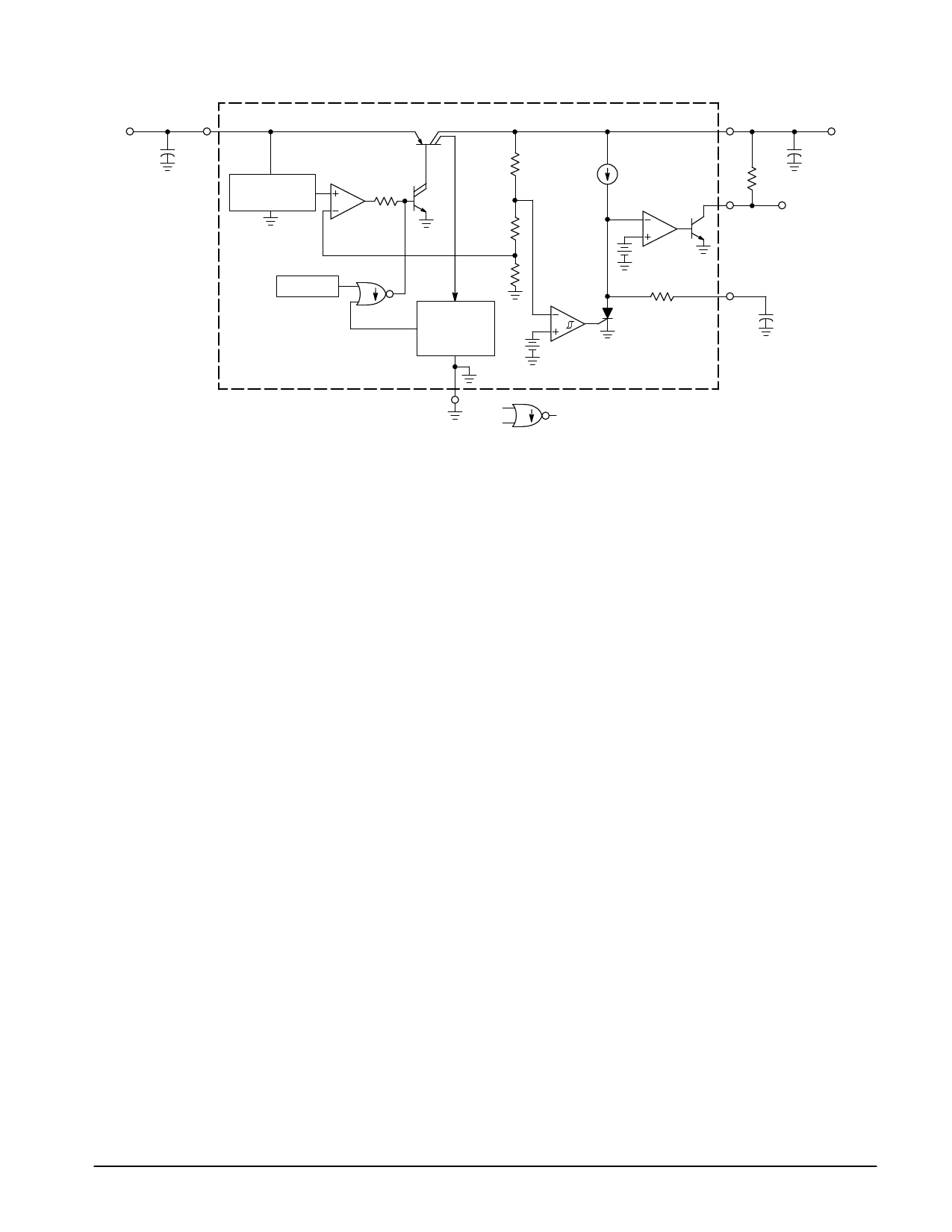
Figure 1. Typical Application Circuit
Input
Vin
Cin
+
0.1
1
Reference
1.25 V
Thermal
3.01
R
20 µA
0.03
R
R
Delay
Overcurrent
Detector
+
1.25 V
Reset
+
3.8 V
200
Ground 3
=
Sink Only
Positive True Logic
Output
5
+
VO
CO 100
Reset
Output
2
Delay
4
+
CDLY
APPLICATION CIRCUIT INFORMATION
The MC33267 is a low dropout, positive fixed 5.0 V,
500 mA regulator. Protection features include output current
limiting and thermal shutdown. System protection consists of
an on–chip power–up microprocessor reset circuit.
A typical applications circuit is shown in Figure 1. The input
bypass capacitor (Cin) is recommended if the regulator is
located an appreciable distance (≥ 4″) from the supply input
filter. This will reduce the circuit’s sensitivity to the input line
impedance at high frequencies.
These regulators are not internally compensated and thus
require an external output capacitor (CO) for stability. The
recommended capacitance is 100 µF with an equivalent
series resistance (ESR) of less than 0.3 Ω. A minimum
capacitance of 33 µF with a maximum ESR of 3.0 Ω can be
used in applications where space is a premium, however,
these limits must be observed over the entire operating
temperature range of the regulator circuit.
With economical electrolytic capacitors, cold temperature
operation can pose a serious stability problem. As the
electrolyte freezes, around – 30°C, the capacitance will
decrease and the ESR will increase drastically, causing the
circuit to oscillate. Quality electrolytic capacitors with
extended temperature ranges of – 40°C to + 85°C and
– 55°C to +105°C are readily available. It is suggested that
oven testing of the entire circuit be performed with maximum
load, minimum input voltage, and minimum ambient
temperature.
Figure 2 shows the reset circuit timing relationship. Note
that whenever the regulator’s output is less than 4.9 V, the
delay capacitor (CDLY) is immediately discharged, and the
reset output is held in a low state. As the regulator’s output
voltage increases beyond 4.97 V, the delay comparator will
allow the 20 µA current source to charge CDLY. The reset
output will go to a high state when CDLY crosses the 3.8 V
threshold of the reset comparator. The reset delay time is
controlled by the value selected for CDLY. The required
system reset time is governed by the microprocessor and
usually a reset signal which lasts several machine cycles is
sufficient.
MOTOROLA ANALOG IC DEVICE DATA
3
Share Link: 