TA8030F Ver la hoja de datos (PDF) - Toshiba
Número de pieza
componentes Descripción
Lista de partido
TA8030F Datasheet PDF : 13 Pages
| |||
TA8030S/F
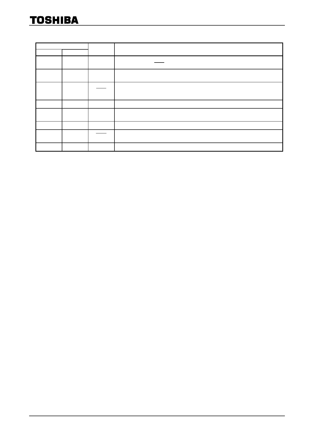
PIN DESCRIPTION
PIN No.
TA80305 TA8030F
1
1
2
2
3
3
4
4
5
6
6
7
7
8
―
5
SYMBOL
DESCRIPTION
WD
TC
RST1
GND
ADJ
VCC
RST2
NC
Clock input pin for watchdog timer. If this IC is only used as a power-on reset timer, this
pin is connected to RST1 .
Time setting pin for the reset and watchdog timers. R1 leads to VCC, and C1 leads to
GND.
Supplies an NPN transistor open-collector output.
● Generates a reset signal determined by the CR combination connected to the TC pin.
● Supplies reset pulses intermittently if no clock is given to the WD pin.
Grounded
VCC detect voltage (1) adjusting pin. The detection voltage is 4.6V when this pin is
grounded ; it is 3.5V when this pin is directly connected to VCC.
Power supply pin for internal circuit. The output voltage can also be detected at this pin.
Supplies an NPN transistor open-collector output. It is the output pin for VCC detect
voltage (2) . The detect voltage has a hysteresis of 0.17V.
Not connected pin.(Electrically,this pin is completely open.)
3
2002-02-27
Share Link: 