70P2352-IGT Ver la hoja de datos (PDF) - Teridian Semiconductor Corporation
Número de pieza
componentes Descripción
Lista de partido
70P2352-IGT Datasheet PDF : 42 Pages
| |||
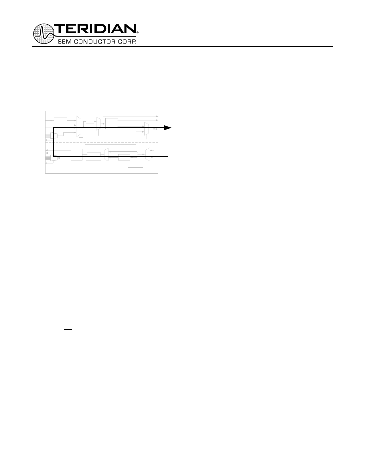
In SW mode only, a Full Remote (digital) Loopback
bit FLBK is also available in the Advanced Tx
Control register. This loopback exercises the entire
Rx and Tx paths of the 78P2352 including the Tx
clock recovery unit. As such, the user must enable
either Serial Plesiochronous or Serial Loop-timing
transmit modes to utilize the Full Remote (digital)
Loopback.
SIxDP/N
SIxCKP/N
PIxCK
PIx[3:0]D
PTOxCK
Lock Detect
Tx CDR
EACH CHANNEL: Tx
FIFO
CMI
Encoder
PMOD, SMOD[1:0], PAR
ECLxP/N
TXxCKP/N
CMIxP/N
RLBK
SOxCKP/N
SOxDP/N
POx[3:0]D
POxCK
CMI
Decoder
Rx CDR
Lock Detect
CMI
EACH CHANNEL: Rx
Adaptive
Eq.
LOS Detect
LLBK
Figure 8: Remote (Digital) Loopback
RXxP/N
INTERNAL POWER-ON RESET
Power-On Reset (POR) function is provided on chip.
Roughly 50µs after Vcc reaches 2.4V at power up, a
reset pulse is internally generated. This resets all
registers to their default values as well as all state
machines within the transceiver to known initial
values. The reset signal is also brought out to the
PORB pin. The PORB pin is a special function
analog pin that allows for the following:
• Override the internal POR signal by driving in
an external active low reset signal;
• Use the internally generated POR signal to
trigger other resets;
• Add external capacitor to slow down the
release of power-on reset (approximately 8µs
per nF added).
NOTE: Do not pull-up the PORB pin to Vcc or drive
this pin high during power-up. This will prevent the
internal reset generator from resetting the entire chip
and may result in errors.
78P2352
Dual Channel
OC-3/ STM1-E/ E4 LIU
SERIAL CONTROL INTERFACE
The serial port controlled registers allows a generic
controller to interface with the 78P2352. It is used
for mode settings, diagnostics and test, retrieval of
status and performance information, and for on-chip
fuse trimming during production test. The SPSL pin
must be high in order to use the serial port.
The serial interface consists of four pins: Serial Port
Enable (SEN_CMI), Serial Clock (SCK_MON), Serial
Data In (SDI_PAR), and Serial Data Out (SDO_E4).
The SEN_CMI pin initiates the read and write
operations. It can also be used to select a
particular device allowing SCK_MON, SDI_PAR
and SDO_E4 to be bussed together.
SCK_MON is the clock input that times the data
on SDI_PAR and SDO_E4. Data on SDI_PAR
is latched in on the rising-edge of SCK_MON,
and data on SDO_E4 is clocked out using the
falling edge of SCK_MON.
SDI_PAR is used to insert mode, address, and
register data into the chip. Address and Data
information are input least significant bit (LSB)
first. The mode and address bit assignment and
register table are shown in the following section.
SDO_E4 is a tri-state capable output. It is used
to output register data during a read operation.
SDO_E4 output is normally high impedance,
and is enabled only during the duration when
register data is being clocked out. Read data is
clocked out least significant bit (LSB) first.
If SDI_PAR coming out of the micro-controller chip is
also tri-state capable, SDI_PAR and SDO_E4 can
be connected together to simplify connections. The
maximum clock frequency for register access is
20MHz.
PROGRAMMABLE INTERRUPTS
In addition to the receiver LOS and LOL status pins,
the 78P2352 provides a programmable interrupt for
each transmitter.
In HW control mode, the default events that trigger
the Tx interrupt is a transmit Loss of Lock (TXLOL)
or FIFO error (FERR).
Page: 8 of 42
2006 Teridian Semiconductor Corporation
Rev. 2.4
Share Link: 