PI6C2308A Ver la hoja de datos (PDF) - Pericom Semiconductor
Número de pieza
componentes Descripción
Lista de partido
PI6C2308A Datasheet PDF : 10 Pages
| |||
PI6C2308A
3.3V Zero Delay Buffer 1122334455667788990011223344556677889900112233445566778899001122112233445566778899001122334455667788990011223344556677889900112211223344556677889900112233445566778899001122334455667788990011221122334455667788990011223344556677889900112233445566778899001122112233445566778899001122
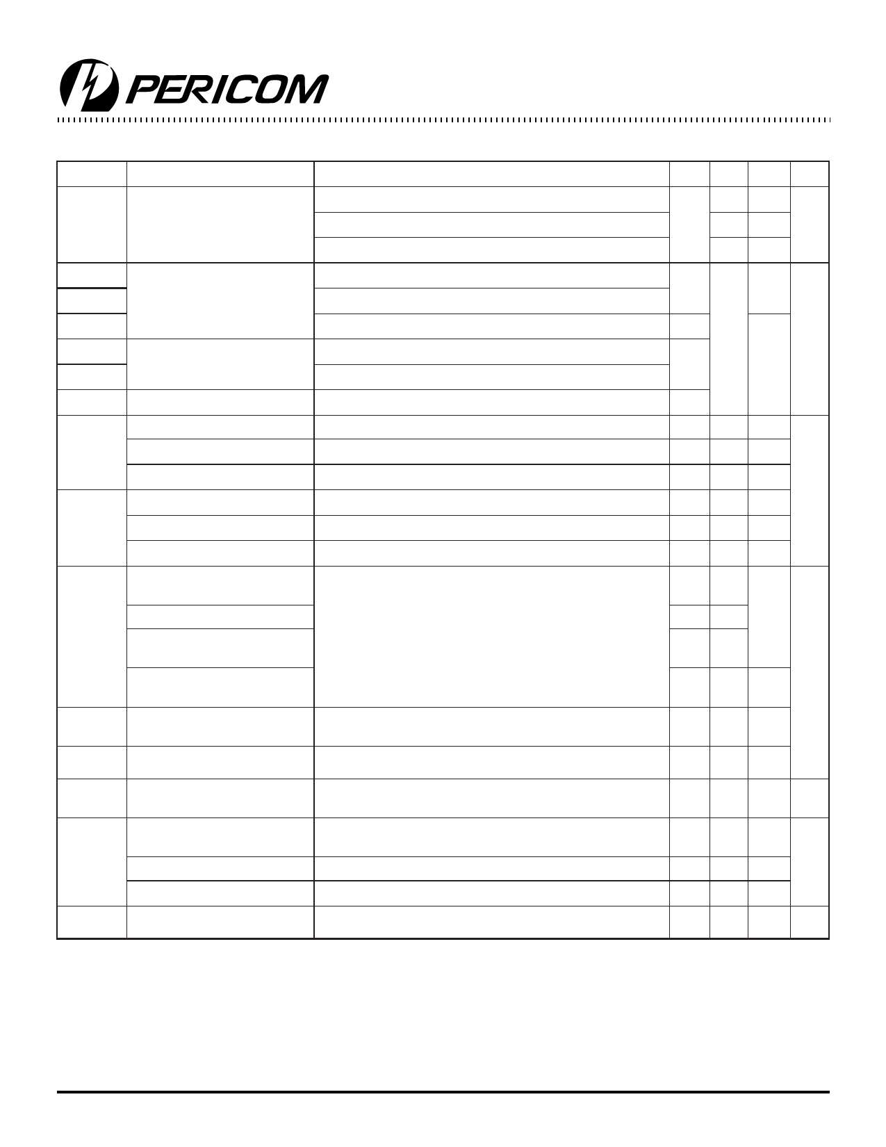
Switching Characteristics for Industrial Temperature Devices(5)
Parameter
Name
Test Conditions
30pF load, All devices
t1
Output Frequency
20pF load, 1H, 5, devices
15pF load, 1,2,3,4 devices
t2
Duty Cycle(4) = t2 ÷ t1
(1,2,3,4)
Measured at 1.4V, FOUT <66.66MHz 30-pF load
Measured at 1.4V, FOUT <100 MHz 15-pF load
Measured at 1.4V, FOUT <133 MHz 15-pF load
Duty Cycle(4) = t2 ÷ t1 (1H,5)
Duty Cycle(4) = t2 ÷ t1 (1H,5)
Rise Time(4) (1,2,3,4)
Measured at 1.4V, FOUT < 45MHz
Measured at 1.4V, FOUT <66.66 MHz 15-pF load
Measured at 1.4V, FOUT <45MHz
Measured between 0.8V and 2.0V, 30-pF load
t3
Rise Time(4) (1,2,3,4)
Rise Time(4) (1H,5)
Measured between 0.8V and 2.0V, 15-pF load
Measured between 0.8V and 2.0V, 30-pF load
Fall Time(4) (1,2,3,4)
Measured between 0.8V and 2.0V, 30-pF load
t4
Fall Time(4) (1,2,3,4)
Fall Time(4) (1H,5)
Measured between 0.8V and 2.0V, 15-pF load
Measured between 0.8V and 2.0V, 30-pF load
Output to Output Skew on same
Bank (1,2,3,4)(4)
Output to Output Skew (1H,5)
t5
Output Bank A to Output Bank B All outputs equally loaded
Skew (1, 4, 5)
Output Bank A to Output Bank B
Skew (2, 3)
t6
Delay, REF Rising Edge to FBK
Rising Edge(4)
Measured at VDD/2
t7
Device to Device Skew(4)
Measured at VDD/2 MHz, on the FBK pins of devices
t8
Output Slew Rate(4)
Measured twx 0.8V & 2.0V on
1H,5 device using Test Circuit #2.
Cycle to Cycle Jitter(4),
(1, 1H,5, 4)
Measured at 66.67 MHz, loaded outputs, 30pF Load
tJ
Cycle to Cycle Jitter(4), (2,3) Measured at 66.67 MHz, loaded outputs, 15pF Load
Cycle to Cycle Jitter(4), (2,3) Measured at 66.67 MHz, loaded outputs
tLOCK PLL Lock Time(4)
Stable power supply, valid clocks presented on REF and FBK pins
Min. Typ. Max. Units
100
10
140 MHz
140
40.0
60.0
35.0
50.0
%
40.0
55.0
45.0
2.2
1.50
1.50
ns
2.50
1.50
1.25
200
ps
400
0 ±150
500
1
V/ns
200
100 ps
400
1.0 ms
Notes:
1. Weak pull-down.
2. Weak pull-down on all outputs.
3. Weak pull-ups on these inputs.
4. REF and FBK inputs have a threshhold voltage of VDD/2.
5. Parameter is guaranteed by design and characterization. Not 100% tested in production.
6. For definition of t1-8, see Switching Waveforms on page 6
7
PS8385B 08/03/00
Share Link: 