UPC8106TB Ver la hoja de datos (PDF) - NEC => Renesas Technology
Número de pieza
componentes Descripción
Lista de partido
UPC8106TB
NEC => Renesas Technology

UPC8106TB Datasheet PDF : 24 Pages
| |||
µPC8106TB, µPC8109TB
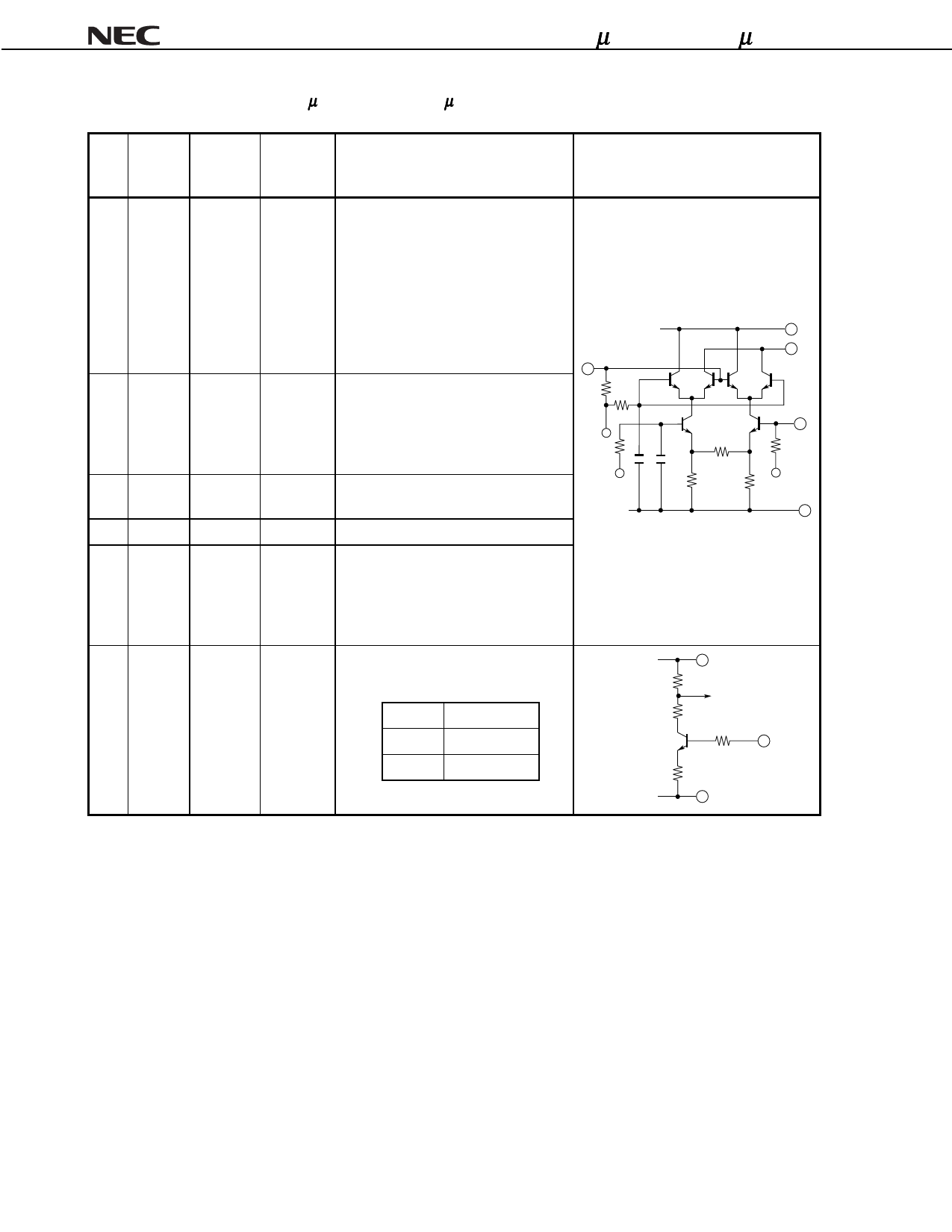
PIN FUNCTIONS (FOR THE µPC8106TB AND µPC8109TB)
Pin
Pin
No. Name
1 IFinput
Applied
Voltage
(V)
−
Pin
Voltage
(V)Note
1.3
2
GND
0
−
3 LOinput
−
2.4
5
VCC
2.7 to 5.5
−
6 RFoutput Same bias
−
as VCC
through
external
inductor
4
PS VCC/GND
−
Function and Explanation
This pin is IF input to double balanced
mixer (DBM). The input is designed as
high impedance. The circuit contri-
butes to suppress spurious signal.
Also this symmetrical circuit can keep
specified performance insensitive to
process-condition distribution. For
above reason, double balanced mixer
is adopted.
3
GND pin. Ground pattern on the board
should be formed as wide as possible.
Track Length should be kept as short
as possible to minimize ground
impedance.
Local input pin. Recommendable input
level is −10 to 0 dBm.
Supply voltage pin.
This pin is RF output from DBM. This
pin is designed as open collector. Due
to the high impedance output, this pin
should be externally equipped with LC
matching circuit to next stage.
Power save control pin. Bias controls
operation as follows.
Pin bias
VCC
GND
Control
Operation
Power Save
Equivalent Circuit
5
6
1
2
VCC
5
4
GND
2
Note Each pin voltage is measured with VCC = VPS = VRFout = 3.0 V.
4
Data Sheet P12770EJ2V0DS00
Share Link: