UPC8128TA Ver la hoja de datos (PDF) - NEC => Renesas Technology
Número de pieza
componentes Descripción
Lista de partido
UPC8128TA
NEC => Renesas Technology

UPC8128TA Datasheet PDF : 16 Pages
| |||
PPC8128TA, PPC8151TA, PPC8152TA
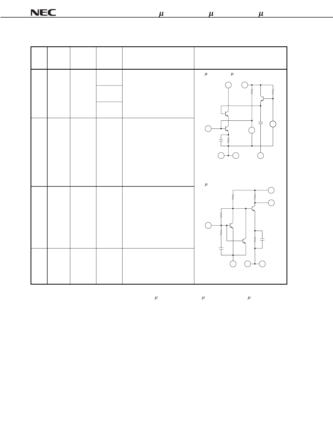
PIN EXPLANATION
Pin Pin
Applied
No.
Name
Voltage
(V)
1
INPUT
ð
Pin
Voltage
(V)Note
0.9
1.06
0.80
Function and Applications
Signal input pin. A internal
matching circuit, configured with
resistors, enables 50 : connec-
tion over a wide band. This pin
must be coupled to signal source
with capacitor for DC cut.
2
GND
0
3
5
ð
Ground pin. This pin should be
connected to system ground with
minimum inductance. Ground
pattern on the board should be
formed as wide as possible.
All the ground pins must be con-
nected together with wide ground
pattern to decrease impedance
defference.
4 OUTPUT voltage
as same
as VCC
through
external
inductor
ð
Signal output pin. This pin is de-
signed as collector output. Due
to the high impedance output,
this pin should be externally
equipped with LC matching
circuit to next stage. For L, a
size 1005 chip in-ductor can be
chosen.
6
VCC
2.4 to 3.3
ð
Power supply pin. This pin
should be externally equipped
with bypass capacitor to
minimize its inpedance.
Internal Equivalent Circuit
µPC8128TA, µPC8151TA
4
6
↓
1
↓
2
5
3
µPC8152TA
6
4
1
3
2
5
Note Pin voltage is measured at VCC = 3.0 V. Above: PPC8128TA, Center: PPC8151TA, Below: PPC8152TA
4
Preliminary Data Sheet P14637EJ1V0DS00
Share Link: