74ACT373 Ver la hoja de datos (PDF) - ON Semiconductor
Número de pieza
componentes Descripción
Lista de partido
74ACT373 Datasheet PDF : 12 Pages
| |||
MC74AC373, MC74ACT373
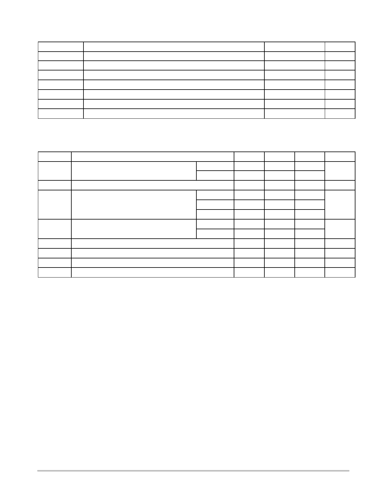
MAXIMUM RATINGS*
Symbol
Parameter
Value
Unit
VCC
VIN
VOUT
IIN
IOUT
ICC
Tstg
DC Supply Voltage (Referenced to GND)
DC Input Voltage (Referenced to GND)
DC Output Voltage (Referenced to GND)
DC Input Current, per Pin
DC Output Sink/Source Current, per Pin
DC VCC or GND Current per Output Pin
Storage Temperature
–0.5 to +7.0
V
–0.5 to VCC +0.5
V
–0.5 to VCC +0.5
V
±20
mA
±50
mA
±50
mA
–65 to +150
°C
*Maximum Ratings are those values beyond which damage to the device may occur. Functional operation should be restricted to the
Recommended Operating Conditions.
RECOMMENDED OPERATING CONDITIONS
Symbol
Parameter
Min
Typ
Max
VCC
Supply Voltage
′AC
′ACT
2.0
5.0
6.0
4.5
5.0
5.5
VIN, VOUT DC Input Voltage, Output Voltage (Ref. to GND)
tr, tf
Input Rise and Fall Time (Note 1)
′AC Devices except Schmitt Inputs
tr, tf
Input Rise and Fall Time (Note 2)
′ACT Devices except Schmitt Inputs
TJ
Junction Temperature (PDIP)
TA
Operating Ambient Temperature Range
IOH
Output Current – High
IOL
Output Current – Low
0
VCC @ 3.0 V
–
VCC @ 4.5 V
–
VCC @ 5.5 V
–
VCC @ 4.5 V
–
VCC @ 5.5 V
–
–
–40
–
–
–
VCC
150
–
40
–
25
–
10
–
8.0
–
–
140
25
85
–
–24
–
24
1. VIN from 30% to 70% VCC; see individual Data Sheets for devices that differ from the typical input rise and fall times.
2. VIN from 0.8 V to 2.0 V; see individual Data Sheets for devices that differ from the typical input rise and fall times.
Unit
V
V
ns/V
ns/V
°C
°C
mA
mA
http://onsemi.com
3
Share Link: 