RF2483 Ver la hoja de datos (PDF) - RF Micro Devices
Número de pieza
componentes Descripción
Lista de partido
RF2483 Datasheet PDF : 34 Pages
| |||
RF2483
Pin Function Description
Interface Schematic
13
QSIG P
Quadrature Q channel positive baseband input port.
Best performance is achieved when the ISIGP and ISIGN are driven differ-
entially. The recommended CW differential drive level (VQSIGP-VQSIGN) is
800 mVP-P.
This input should be DC-biased at 1.2V±0.05V. The common-mode DC
voltage on the QSIGP and QSIGN input signals is used to bias the modula-
tor. In sleep mode an internal FET switch is opened, the input goes high
impedance and the modulator is de-biased. The input impedance is typi-
V CC2
cally 5.5k at low frequencies and at higher frequencies can be modeled
as 50 in series with 12pF to ground.
50
Phase or amplitude errors between the QSIGP and QSIGN signals which
may result in an increase in the even order distortion of the modulation in
the output spectrum.
12 pF
DC offsets between the QSIGP and QSIGN signals will result in an
increased carrier leakage. Small DC offsets may be deliberately applied
between the ISIGP/ISIGN and QSIGP/QSIGN inputs to cancel out the LO
leakage. The optimum corrective DC offsets will change with mode, fre-
quency and gain control.
Common-mode noise on the QSIGP and QSIGN should be kept low as it
may degrade the noise performance of the modulator.
Phase offsets may be applied between the I and Q channels to improve the
sideband suppression performance.
14
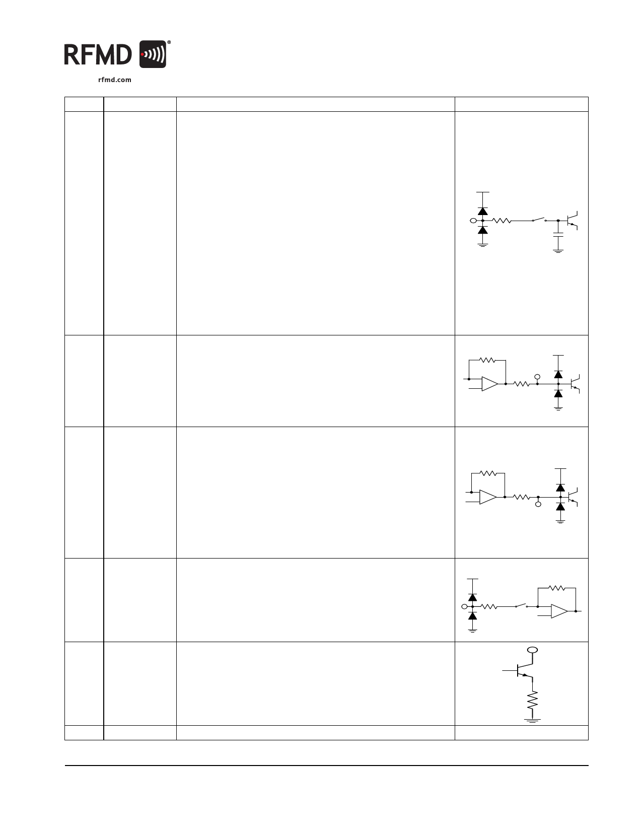
VREF
Voltage reference decouple with an external 10nF capacitor to ground.
The voltage on this pin is typically 1.67V when the chip is enabled. The
4 k
VCC2
voltage is 0V when the chip is powered down.
The purpose of this decoupling capacitor is to filter out low frequency noise
(20MHz) on the gain control lines.
-
+
Poor positioning of the VREF decoupling capacitor can cause a degrada-
tion in LO leakage.
A voltage of around 2.5V on this pin indicates that the die flag under the
chip is not grounded and the chip is not biased correctly.
15
GC DEC
Voltage reference decouple with an external 1nF decoupling capacitor to
ground.
The voltage on this pin is a function of gain control (GC) voltage when the
chip is enabled. The voltage is 0V when the chip is powered down.
4 k
VCC2
The purpose of this decoupling capacitor is to filter out low frequency noise
(20MHz) on the gain control lines. The size of the capacitor on the GC DEC
line will effect the settling time response to a change in gain control volt-
+
age. A 1nF capacitor equates to around 200ns settling time and a 0.5nF
-
capacitor equates to a 100ns settling time. There is a trade-off between
settling time and noise contributions by the gain control circuitry as gain
control is applied.
Poor positioning of the VREF decoupling capacitor can cause a degrada-
tion in LO leakage.
16
GC
Gain control voltage. Maximum output power at 2.0V. Minimum output
power at 0V. When the chip is enabled the input impedance is 10k refer- VCC2
enced to 1.7VDC. When the chip is powered down a FET switch is opened
4 k
and the input goes high impedance.
10 k
-
1.7 V +
17
RF OUT LB RF low band output. Open collector output.
The output should be biased at VCC through an inductor that can be used
to form part of an output matching circuit.
In our proposed applications circuit some power is dissipated in R6 (130)
which appears as a de-Qing resistor in parallel with the output inductor L4.
If R6 is eliminated and the RFOUT LB pin is re-matched to 50 it is possi-
ble to get approximately 5dB extra power out of the device in low band
mode.
18
GND2
Ground for RF output sections.
DS110505
7628 Thorndike Road, Greensboro, NC 27409-9421 · For sales or technical
support, contact RFMD at (+1) 336-678-5570 or sales-support@rfmd.com.
11 of 34
Share Link: 