RF2483PCBA-41X(V2) Ver la hoja de datos (PDF) - RF Micro Devices
Número de pieza
componentes Descripción
Lista de partido
RF2483PCBA-41X Datasheet PDF : 28 Pages
| |||
RF2483
Pin
19
20
Die
Flag
Function
RF OUT HB
GND3
GND4
Description
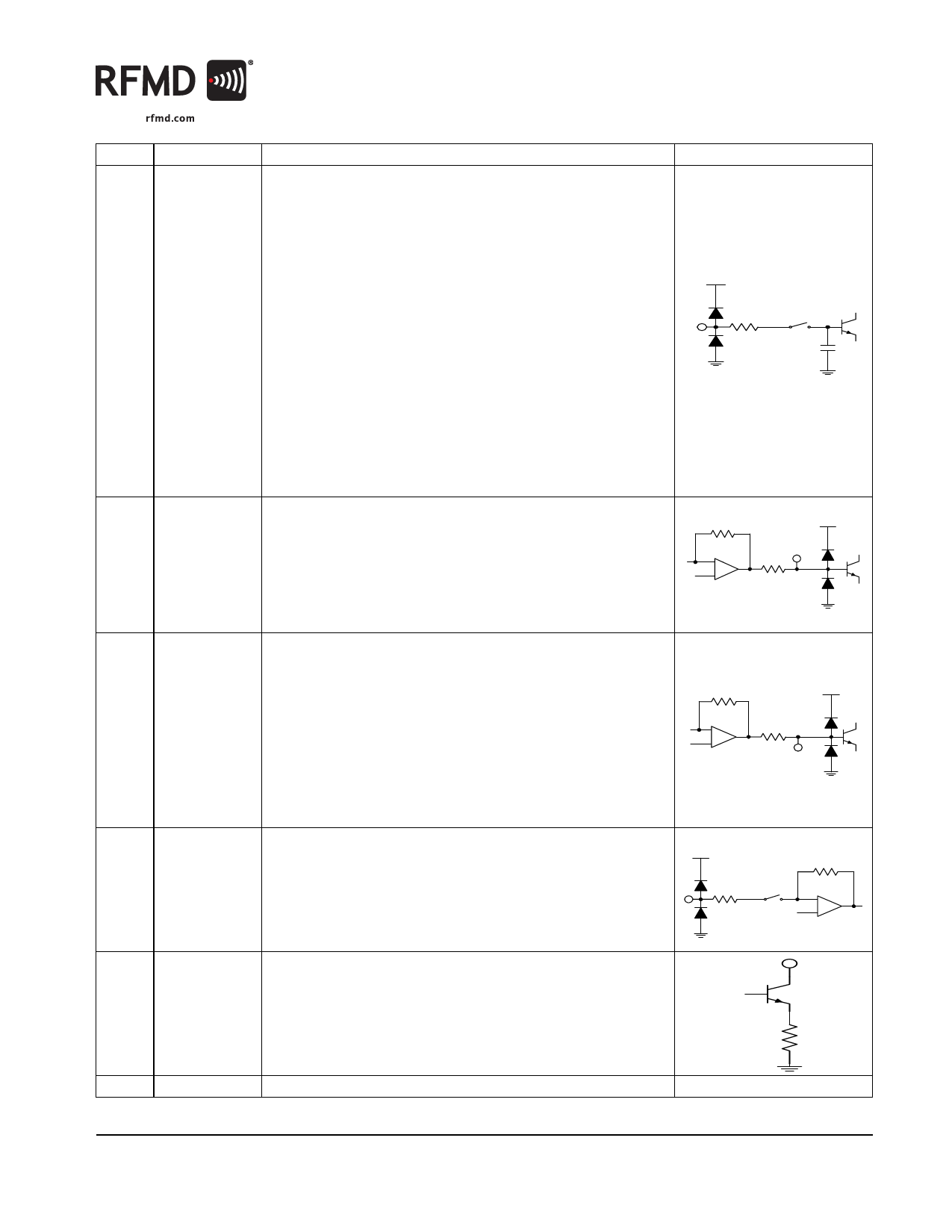
Interface Schematic
RF high band output. Open collector output.
The output should be biased at VCC through an inductor that can be used
to form part of an output matching circuit.
In our proposed applications circuit some power is dissipated in R4 (180Ω)
which appears as a de-Qing resistor in parallel with the output inductor L3.
If R4 is eliminated and the RFOUT HB pin is re-matched to 50Ω it is possi-
ble to get approximately 3dB extra power out of the device in high band
mode.
Ground for RF output sections.
Ground for modulator, variable gain amplifier and substrate.
Package Drawing
-A-
4.00 SQ.
0.10 C A
2 PLCS
2.00 TYP
0.10 C B
2 PLCS
0.90
0.85
0.05
0.00
0.05 C
0.70
0.65
0.10 C B
2 PLCS
0.10 C A
2 PLCS
3.75 SQ.
-B-
1.87 TYP
Dimensions in m m.
NOTES:
1. Shaded lead is Pin 1.
2 Dim ension applies to plated term inal:
to be measured between 0.20 mm and 0.25 mm
from terminal end.
0.60
0.24
TYP
0.75
0.50
TYP
12°
MAX
SEATING
PLANE
-C -
0.10 M C A B
0.30
0.18
2
PIN 1
ID
0.20 R
2.2
1.9
5
5
S
Q
.
0.50
Rev A8 DS060203
7628 Thorndike Road, Greensboro, NC 27409-9421 · For sales or technical
support, contact RFMD at (+1) 336-678-5570 or sales-support@rfmd.com.
11 of 28
Share Link: 