RF2483 Ver la hoja de datos (PDF) - RF Micro Devices
Número de pieza
componentes Descripción
Lista de partido
RF2483 Datasheet PDF : 34 Pages
| |||
RF2483
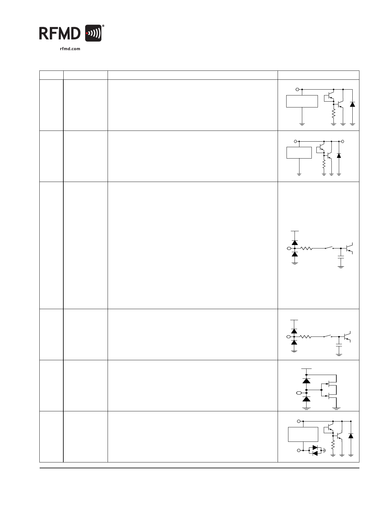
Pin Names and Descriptions
Pin Function Description
1
VCC3
Supply for RF output circuits.
Interface Schematic
VCC3
RF Output
Amplifier
2
VCC2
Supply for modulator and biasing circuits.
VCC2
Modulator and
VGA
VCC2
3
ISIG P
In phase I channel positive baseband input port. Best performance is
achieved when the ISIGP and ISIGN are driven differentially. The recom-
mended CW differential drive level (VISIGP-VISIGN) is 800mVP-P.
This input should be DC-biased at 1.2V±0.05V. The common-mode DC
coltage on the ISIGP and ISIGN input signals is used to bias the modulator.
In sleep mode an internal FET switch is opened, the input goes high imped-
ance and the modulator is de-biased. The input impedance is typically
5.5k at low frequencies and at higher frequencies can be modeled as
V CC2
50 in series with 12pF to ground.
Phase or amplitude errors between the ISIGP and ISIGN signals may result
50
in the even order distortion of the modulation in the output spectrum.
DC offsets between the ISIGP and ISIGN signals will result in increased car-
rier leakage. Small DC offsets may be deliberately applied between the
12 pF
ISIGP/ISIGN and QSIGP/QSIGN inputs to cancel out LO leakage. The opti-
mum corrective DC offsets will change with mode, frequency and gain con-
trol.
Common-mode noise on the ISIGP and ISGN should be kept low as it may
degrade the noise performance of the modulator.
Phase offsets may be applied between the I and Q channels to improve the
sideband suppression performance.
4
ISIG N
In phase I channel negative baseband input port. See ISIGP.
V CC2
50
12 pF
5
ENABLE Enables power to the device.
CMOS input.
Logic 1 (1.4V to VCC)=Enabled.
Logic 0 (0V to 0.5V)=Powered Down.
V CC2
6
VCC1
Supply for the LO buffers and quadrature network.
The sideband suppression is a function of the VCC1 voltage. The inclusion VCC1
of R3 (39) lowers the voltage on VCC1 by around 400mV and results an
improvement in sideband suppression but around a 0.2dB increase in
LO Quadrature
Generator and
noise at 20MHz offset.
Buffers
GND1
DS110505
7628 Thorndike Road, Greensboro, NC 27409-9421 · For sales or technical
support, contact RFMD at (+1) 336-678-5570 or sales-support@rfmd.com.
9 of 34
Share Link: 