LB1662D Ver la hoja de datos (PDF) - SANYO -> Panasonic
Número de pieza
componentes Descripción
Lista de partido
LB1662D Datasheet PDF : 6 Pages
| |||
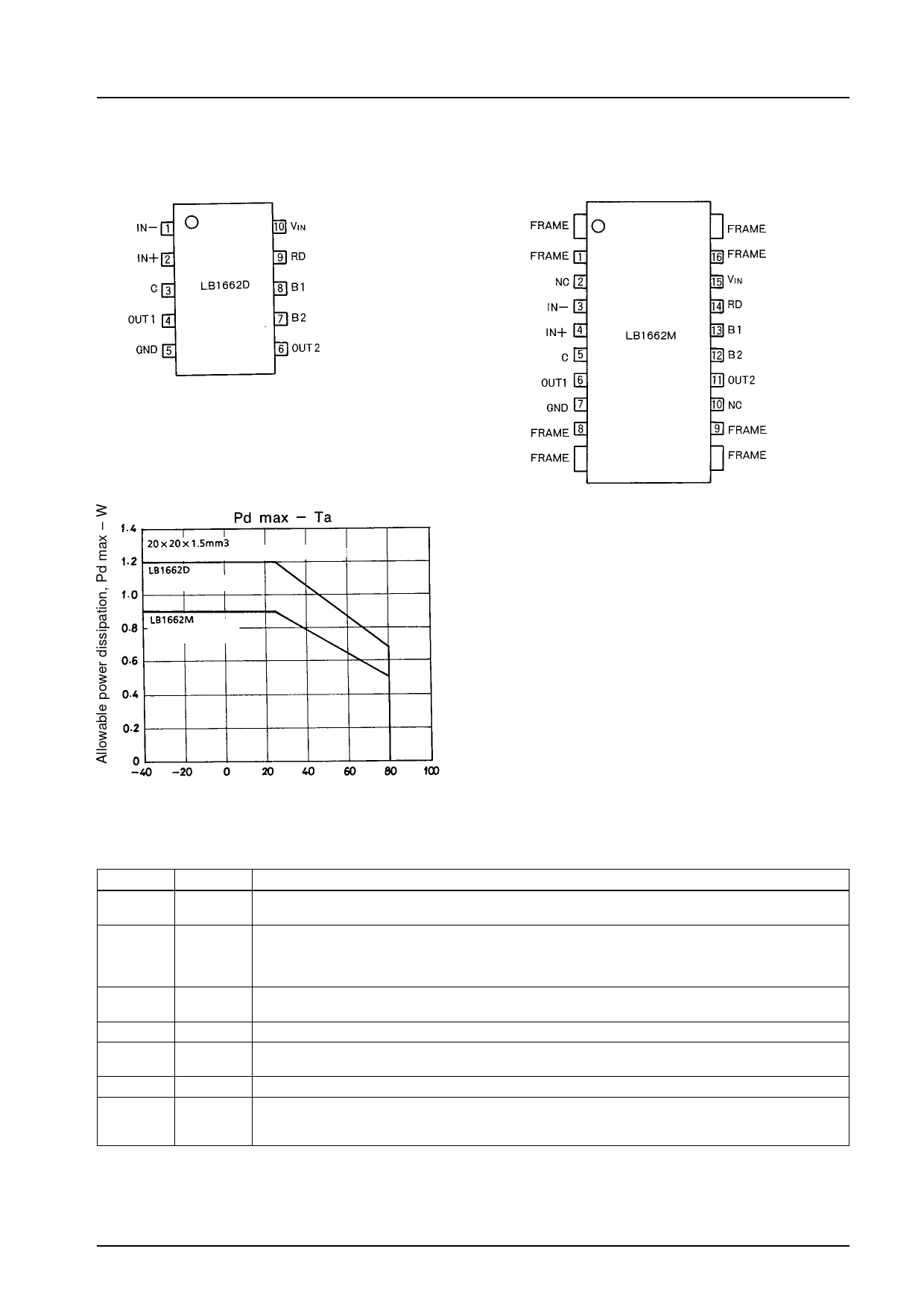
Pin Assignments
LB1662D, 1662M
Glass epoxy resin (LB1662M)
(Independent IC)
(Independent IC)
Top view
Ambient temperature, Ta – °C
Pin Functions
Pin No.
1
2
3
4
6
5
8
7
9
10
Pin name
IN−
IN+
C
OUT1
OUT2
GND
B1
B2
RD
VIN
Function
Input pins for hall element outputs.
Common-mode input voltage range is 0 to VIN−1.5 V, offset voltage is ±7 mV
Capacitor pin (1 to 10 µF) that forms automatic return circuit.
When rotation is stopped due to overload, the pin voltage increases and output stops.
After proper load adjustment, the output returns from ‘‘stop’’ mode to ‘‘drive’’ mode automatically.
The lock detect time can be set by changing the capacitor constant.
Output pins. The output transistor is Darlington connected.
Connect either an external capacitor or an external Zener diode for output transistor protection.
Ground pin.
Base pins for Darlington connected output transistors.
If radio noise is a problem, add a capacitor (0.01 to 0.1 µF).
Open collector output. Drive mode: ‘‘L’’, Stop mode: ‘‘H’’
Insert a limiting resistor between VCC and VIN and use the voltage applied between VIN and ground in a
range from 3.8 to 6.0 V.
In this case, the current consumption ICC at the VIN pin is 1.4 to 3.7 mA (when VIN = 4.3 V).
No.3416-3/6
Share Link: 