74LVT16646 Ver la hoja de datos (PDF) - Fairchild Semiconductor
Número de pieza
componentes Descripción
Lista de partido
74LVT16646 Datasheet PDF : 9 Pages
| |||
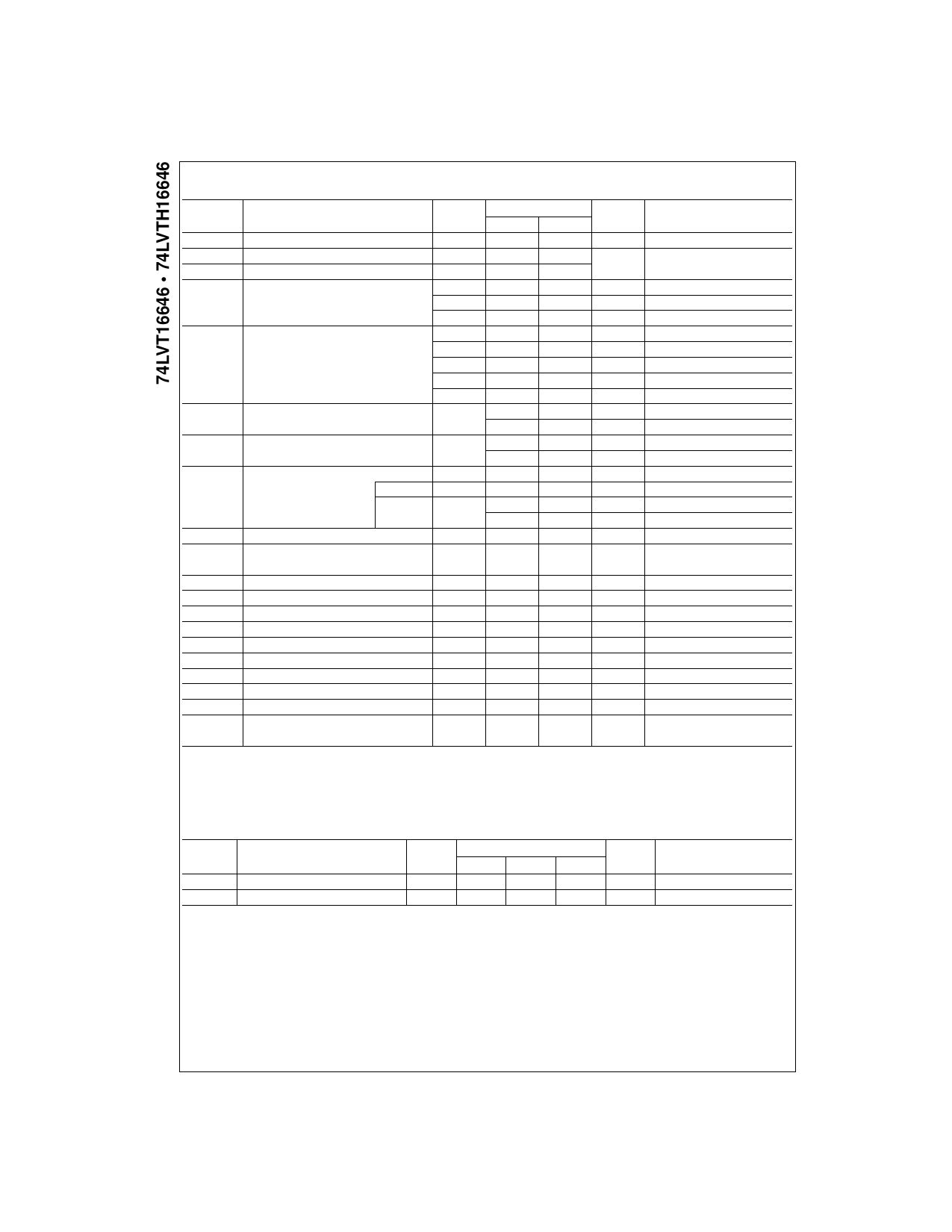
DC Electrical Characteristics
Symbol
Parameter
VCC
T A = −40°C to +85°C
Units
(V)
Min
Max
Conditions
VIK
Input Clamp Diode Voltage
VIH
Input HIGH Voltage
VIL
Input LOW Voltage
VOH
Output HIGH Voltage
VOL
Output LOW Voltage
II(HOLD)
(Note 4)
II(OD)
(Note 4)
Bushold Input Minimum Drive
Bushold Input Over-Drive
Current to Change State
2.7
−1.2
2.7–3.6
2.0
2.7–3.6
0.8
2.7–3.6
2.7
VCC − 0.2
2.4
3.0
2.0
2.7
0.2
2.7
0.5
3.0
0.4
3.0
0.5
3.0
0.55
75
3.0
−75
500
3.0
−500
V
II = −18 mA
V
VO ≤ 0.1V or
VO ≥ VCC − 0.1V
V
IOH = −100 µA
V
IOH = −8 mA
V
IOH = −32 mA
V
IOL = 100 µA
V
IOL = 24 mA
V
IOL = 16 mA
V
IOL = 32 mA
V
IOL = 64 mA
µA
VI = 0.8V
µA
VI = 2.0V
µA
(Note 5)
µA
(Note 6)
II
Input Current
3.6
Control Pins 3.6
Data Pins
3.6
IOFF
IPU/PD
Power Off Leakage Current
Power Up/Down 3-STATE
Output Current
IOZL (Note 4) 3-STATE Output Leakage Current
IOZL
3-STATE Output Leakage Current
IOZH (Note 4) 3-STATE Output Leakage Current
IOZH
3-STATE Output Leakage Current
IOZH+
3-STATE Output Leakage Current
ICCH
Power Supply Current
ICCL
Power Supply Current
ICCZ
Power Supply Current
ICCZ+
Power Supply Current
∆ICC
Increase in Power Supply Current
(Note 7)
Note 4: Applies to bushold version only (74LVTH16646)
0
0–1.5V
3.6
3.6
3.6
3.6
3.6
3.6
3.6
3.6
3.6
3.6
10
±1
−5
1
±100
±100
−5
−5
5
5
10
0.19
5
0.19
0.19
0.2
µA
VI = 5.5V
µA
VI = 0V or VCC
µA
VI = 0V
µA
VI = VCC
µA
0V ≤ VI or VO ≤ 5.5V
µA
VO = 0.5V to 3.0V
VI = GND or VCC
µA
VO = 0.0V
µA
VO = 0.5V
µA
VO = 3.6V
µA
VO = 3.0V
µA
VCC < VO ≤ 5.5V
mA Outputs HIGH
mA Outputs LOW
mA Outputs Disabled
mA
VCC ≤ VO ≤ 5.5V,Outputs Disabled
mA
One Input at VCC − 0.6V
Other Inputs at VCC or GND
Note 5: An external driver must source at least the specified current to switch from LOW-to-HIGH.
Note 6: An external driver must sink at least the specified current to switch from HIGH-to-LOW.
Note 7: This is the increase in supply current for each input that is at the specified voltage level rather than VCC or GND.
Dynamic Switching Characteristics (Note 8)
Symbol
Parameter
VCC
TA = 25°C
Units
(V)
Min
Typ
Max
VOLP
Quiet Output Maximum Dynamic VOL
3.3
0.8
V
VOLV
Quiet Output Minimum Dynamic VOL
3.3
−0.8
V
Note 8: Characterized in SSOP package. Guaranteed parameter, but not tested.
Note 9: Max number of outputs defined as (n). n−1 data inputs are driven 0V to 3V. Output under test held LOW.
Conditions
CL = 50 pF, RL = 500Ω
(Note 9)
(Note 9)
www.fairchildsemi.com
6
Share Link: 