MC14017BCP Ver la hoja de datos (PDF) - ON Semiconductor
Número de pieza
componentes Descripción
Lista de partido
MC14017BCP Datasheet PDF : 8 Pages
| |||
MC14017B
Decade Counter
The MC14017B is a five–stage Johnson decade counter with
built–in code converter. High speed operation and spike–free outputs
are obtained by use of a Johnson decade counter design. The ten
decoded outputs are normally low, and go high only at their
appropriate decimal time period. The output changes occur on the
positive–going edge of the clock pulse. This part can be used in
frequency division applications as well as decade counter or decimal
decode display applications.
• Fully Static Operation
• DC Clock Input Circuit Allows Slow Rise Times
• Carry Out Output for Cascading
• Divide–by–N Counting
• Supply Voltage Range = 3.0 Vdc to 18 Vdc
• Capable of Driving Two Low–power TTL Loads or One Low–power
Schottky TTL Load Over the Rated Temperature Range
• Pin–for–Pin Replacement for CD4017B
• Triple Diode Protection on All Inputs
http://onsemi.com
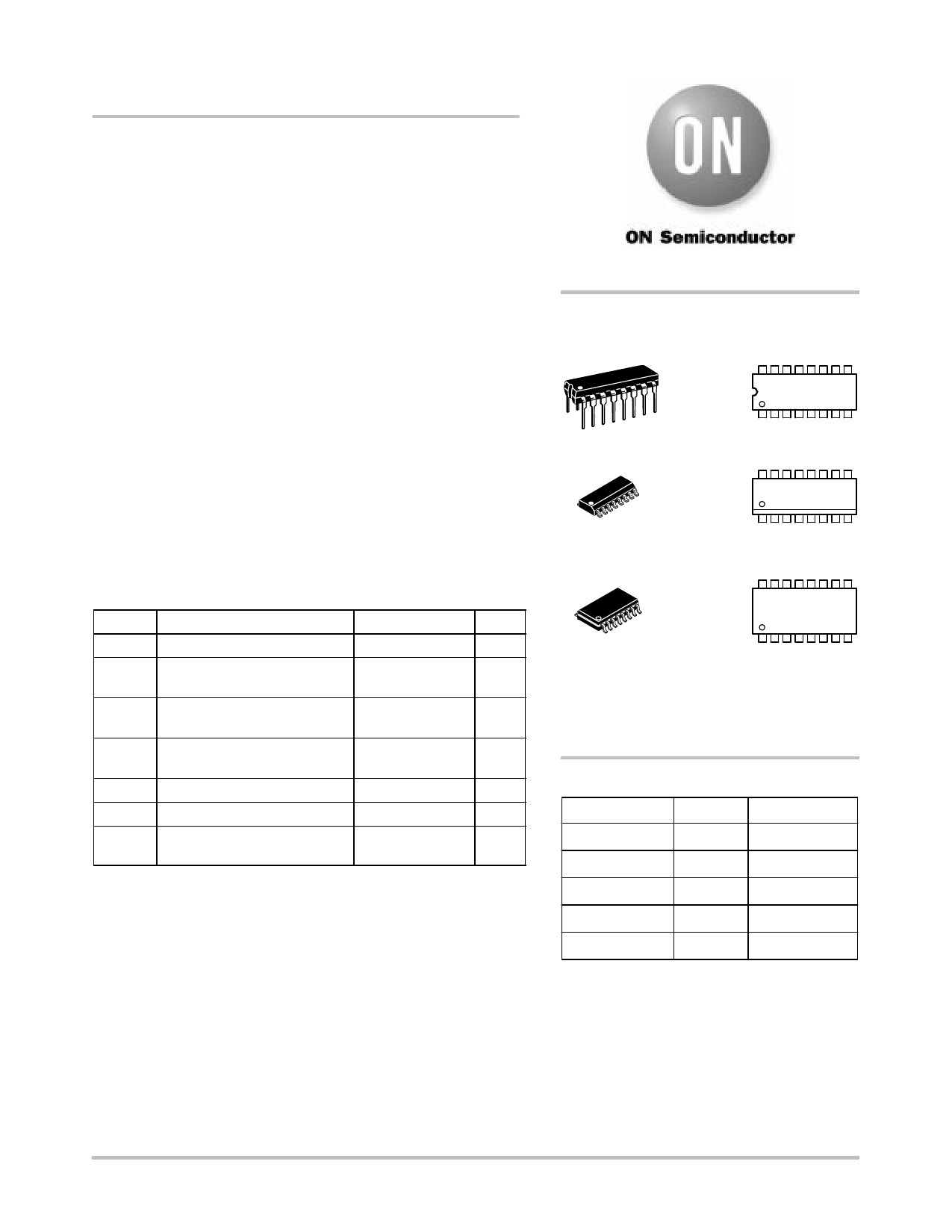
PDIP–16
P SUFFIX
CASE 648
MARKING
DIAGRAMS
16
MC14017BCP
AWLYYWW
1
SOIC–16
D SUFFIX
CASE 751B
16
14017B
AWLYWW
1
MAXIMUM RATINGS (Voltages Referenced to VSS) (Note 2.)
Symbol
Parameter
Value
Unit
VDD
DC Supply Voltage Range
–0.5 to +18.0
V
Vin, Vout Input or Output Voltage Range –0.5 to VDD + 0.5
V
(DC or Transient)
Iin, Iout
Input or Output Current
(DC or Transient) per Pin
±10
mA
PD
Power Dissipation,
per Package (Note 3.)
500
mW
TA
Ambient Temperature Range
Tstg
Storage Temperature Range
TL
Lead Temperature
(8–Second Soldering)
–55 to +125
°C
–65 to +150
°C
260
°C
2. Maximum Ratings are those values beyond which damage to the device
may occur.
3. Temperature Derating:
Plastic “P and D/DW” Packages: – 7.0 mW/_C From 65_C To 125_C
This device contains protection circuitry to guard against damage due to high
static voltages or electric fields. However, precautions must be taken to avoid
applications of any voltage higher than maximum rated voltages to this
high–impedance circuit. For proper operation, Vin and Vout should be constrained
to the range VSS v (Vin or Vout) v VDD.
Unused inputs must always be tied to an appropriate logic voltage level (e.g.,
either VSS or VDD). Unused outputs must be left open.
SOEIAJ–16
F SUFFIX
CASE 966
16
MC14017B
ALYW
1
A
WL, L
YY, Y
WW, W
= Assembly Location
= Wafer Lot
= Year
= Work Week
ORDERING INFORMATION
Device
Package
Shipping
MC14017BCP
PDIP–16
2000/Box
MC14017BD
SOIC–16
48/Rail
MC14017BDR2 SOIC–16 2500/Tape & Reel
MC14017BF
SOEIAJ–16 See Note 1.
MC14017BFEL SOEIAJ–16 See Note 1.
1. For ordering information on the EIAJ version of the
SOIC packages, please contact your local ON
Semiconductor representative.
© Semiconductor Components Industries, LLC, 2000
1
August, 2000 – Rev. 4
Publication Order Number:
MC14017B/D
Share Link: 