74LVC245A Ver la hoja de datos (PDF) - ON Semiconductor
Número de pieza
componentes Descripción
Lista de partido
74LVC245A Datasheet PDF : 9 Pages
| |||
74LVC245A
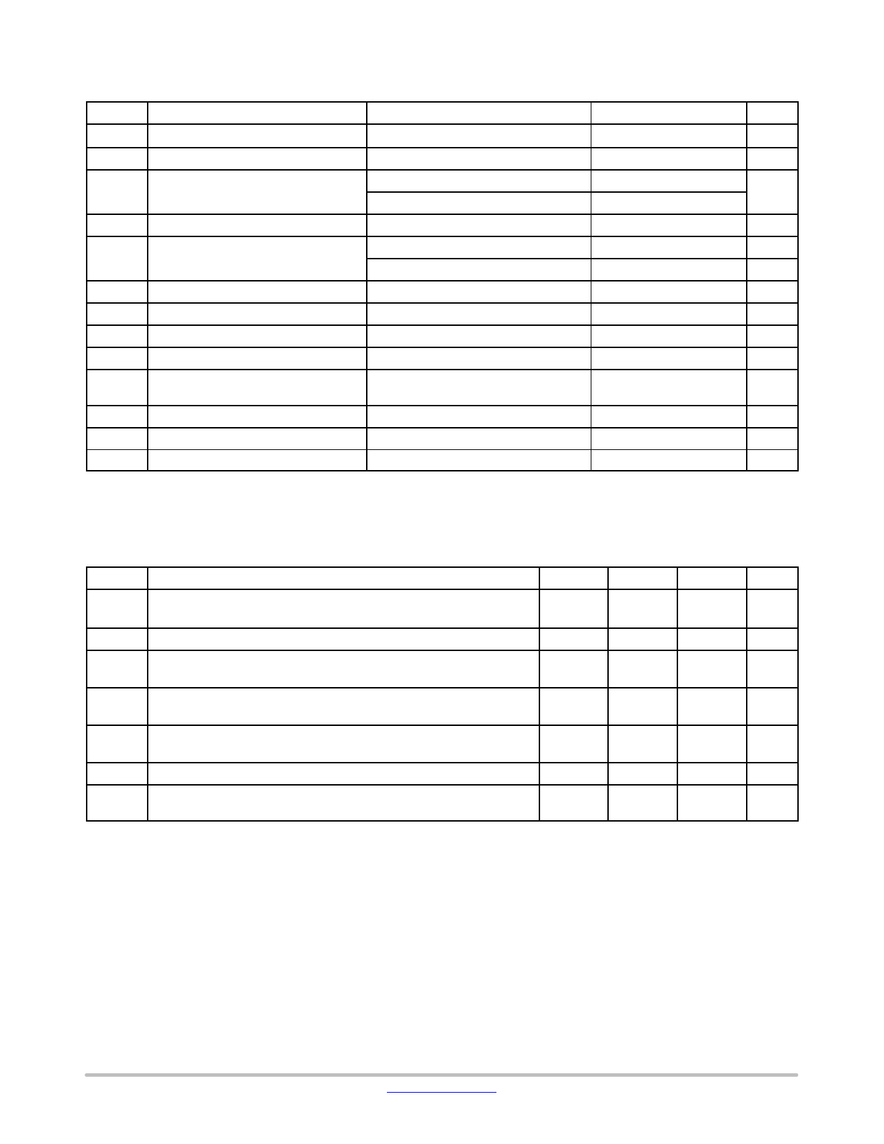
MAXIMUM RATINGS
Symbol
Parameter
Condition
Value
Unit
VCC DC Supply Voltage
−0.5 to +6.5
V
VI
DC Input Voltage
−0.5 ≤ VI ≤ +6.5
V
VO
DC Output Voltage
Output in 3−State
−0.5 ≤ VO ≤ +6.5
V
Output in HIGH or LOW State (Note 1)
−0.5 ≤ VO ≤ VCC + 0.5
IIK
DC Input Diode Current
VI < GND
−50
mA
IOK
DC Output Diode Current
VO < GND
−50
mA
VO > VCC
+50
mA
IO
DC Output Source/Sink Current
±50
mA
ICC
DC Supply Current Per Supply Pin
±100
mA
IGND DC Ground Current Per Ground Pin
±100
mA
TSTG Storage Temperature Range
−65 to +150
°C
TL
Lead Temperature, 1 mm from Case for
10 Seconds
TL = 260
°C
TJ
Junction Temperature Under Bias
TJ = 135
°C
qJA
Thermal Resistance (Note 2)
110.7
°C/W
MSL Moisture Sensitivity
Level 1
Stresses exceeding those listed in the Maximum Ratings table may damage the device. If any of these limits are exceeded, device functionality
should not be assumed, damage may occur and reliability may be affected.
1. IO absolute maximum rating must be observed.
2. Measured with minimum pad spacing on an FR4 board, using 10 mm−by−1 inch, 2 ounce copper trace no air flow.
RECOMMENDED OPERATING CONDITIONS
Symbol
Parameter
VCC Supply Voltage
Min
Typ
Max
Unit
Operating
1.65
Functional
1.2
3.6
V
3.6
VI
Input Voltage
VO
Output Voltage
0
HIGH or LOW State
0
3−State
0
5.5
V
VCC
V
5.5
IOH
HIGH Level Output Current
VCC = 3.0 V − 3.6 V
VCC = 2.7 V − 3.0 V
−24
mA
−12
IOL
LOW Level Output Current
VCC = 3.0 V − 3.6 V
VCC = 2.7 V − 3.0 V
24
mA
12
TA
Operating Free−Air Temperature
−40
+125
°C
Dt/DV Input Transition Rise or Fall Rate
VCC = 1.2 to 2.7 V
0
VCC = 2.7 to 3.6 V
0
20
ns/V
10
Functional operation above the stresses listed in the Recommended Operating Ranges is not implied. Extended exposure to stresses beyond
the Recommended Operating Ranges limits may affect device reliability.
www.onsemi.com
3
Share Link: 