4070M3(2007) Ver la hoja de datos (PDF) - Bourns, Inc
Número de pieza
componentes Descripción
Lista de partido
4070M3 Datasheet PDF : 12 Pages
| |||
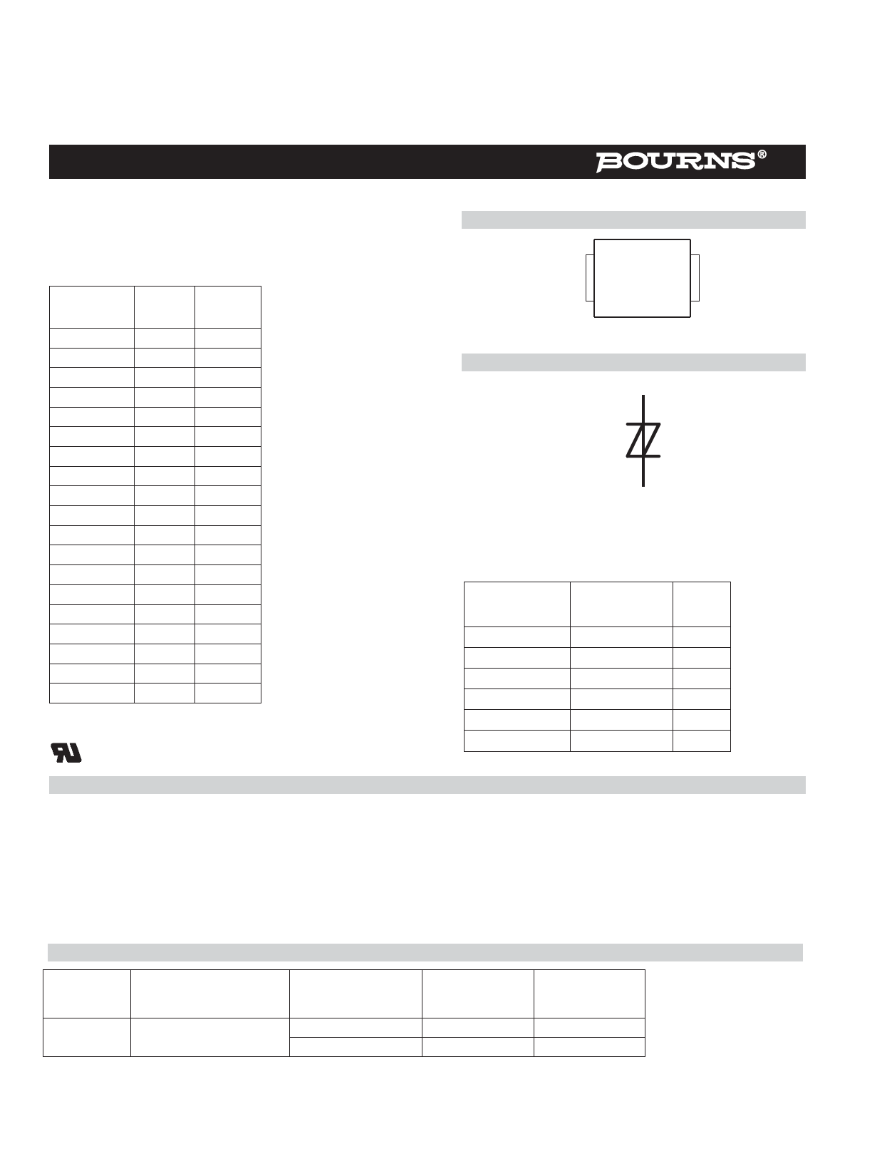
TISP4xxxM3BJ Overvoltage Protector Series
Description (continued)
The TISP4xxxM3BJ range consists of nineteen voltage variants to meet various maximum system voltage levels (58 V to 320 V). They are
guaranteed to voltage limit and withstand the listed international lightning surges in both polarities. These medium (M) current protection
devices are in a plastic package SMBJ (JEDEC DO-214AA with J-bend leads) and supplied in embossed tape reel pack. For alternative
voltage and holding current values, consult the factory. For higher rated impulse currents in the SMB package, the 100 A 10/1000
TISP4xxxH3BJ series is available.
Absolute Maximum Ratings, TA = 25 °C (Unless Otherwise Noted)
Rating
Symbol
Value
Unit
‘4070
± 58
‘4080
± 65
‘4095
± 75
‘4115
± 90
‘4125
±100
‘4145
±120
‘4165
±135
‘4180
±145
‘4200
±155
Repetitive peak off-state voltage, (see Note 1)
‘4220
‘4240
VDRM
±160
V
±180
‘4250
±190
‘4265
±200
‘4290
±220
‘4300
±230
‘4350
±275
‘4360
±290
‘4395
±320
‘4400
±300
Non-repetitive peak on-state pulse current (see Notes 2, 3 and 4)
2/10 µs (GR-1089-CORE, 2/10 µs voltage wave shape)
300
8/20 µs (IEC 61000-4-5,combination wave generator, 1.2/50 voltage, 8/20 current)
220
10/160 µs (FCC Part 68, 10/160 µs voltage wave shape)
120
5/200 µs (VDE 0433, 10/700 µs voltage wave shape)
0.2/310 µs (I3124, 0.5/700 µs voltage wave shape)
110
ITSP
A
100
5/310 µs (ITU-T K.20/21/45, K.44 10/700 µs voltage wave shape)
100
5/310 µs (FTZ R12, 10/700 µs voltage wave shape)
100
10/560 µs (FCC Part 68, 10/560 µs voltage wave shape)
75
10/1000 µs (GR-1089-CORE, 10/1000 µs voltage wave shape)
50
Non-repetitive peak on-state current (see Notes 2, 3 and 5)
20 ms (50 Hz) full sine wave
30
16.7 ms (60 Hz) full sine wave
1000 s 50 Hz/60 Hz a.c.
ITSM
32
A
2.1
Initial rate of rise of on-state current, Exponential current ramp, Maximum ramp value < 100 A
diT/dt
300
A/µs
Junction temperature
TJ
-40 to +150
°C
Storage temperature range
Tstg
-65 to +150
°C
NOTES: 1. See Applications Information and Figure 11 for voltage values at lower temperatures.
2. Initially,the TISP4xxxM3BJ must be in thermal equilibrium with TJ = 25 °C.
3. The surge may be repeated after the TISP4xxxM3BJ returns to its initial conditions.
4. See Applications Information and Figure 12 for current ratings at other temperatures.
5. EIA/JESD51-2 environment and EIA/JESD51-3 PCB with standard footprint dimensions connected with 5 A rated printed wiring
track widths. See Figure 9 for the current ratings at other durations. Derate current values at -0.61 %/°C for ambient temperatures
above 25 ° C.
NOVEMBER 1997 - REVISED MAY 2007
Specifications are subject to change without notice.
Customers should verify actual device performance in their specific applications.
Share Link: 